

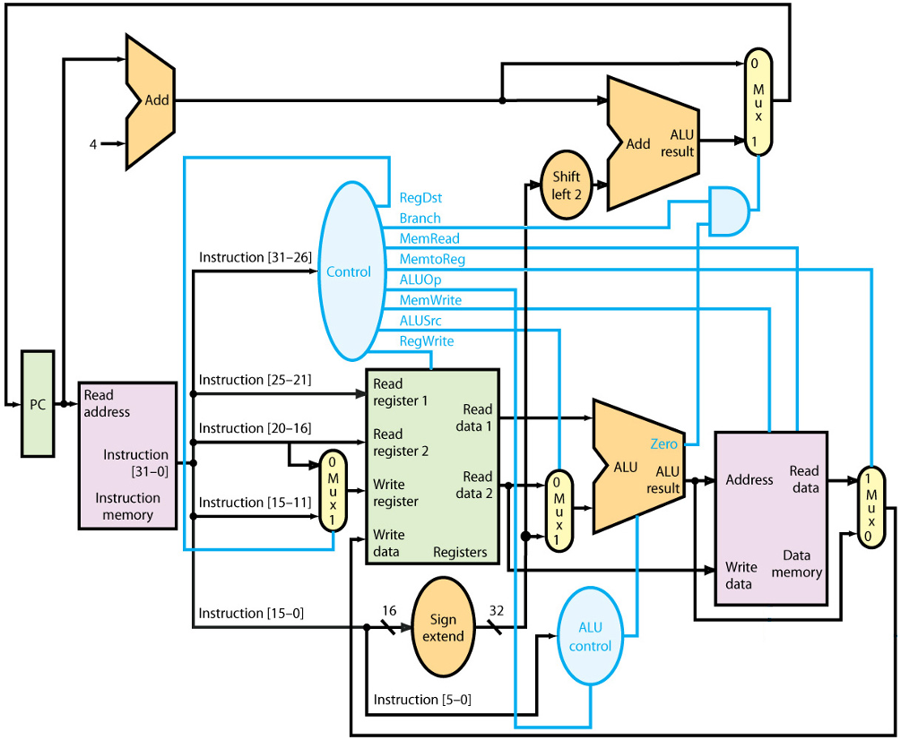
Question: Consider the CPU diagram below, when executing an arbitrary mix of instructions, what is the fastest clock period and clock frequency at which our single
Consider the CPU diagram below, when executing an arbitrary mix of instructions, what is the fastest clock period and clock frequency at which our single cycle CPU could safely operate?
Use the following latencies:
Using the CPU diagram from the start of this assignment, assume that the logic blocks in the processor have the following latencies and constraints:
The PC register will be ready to output data at the beginning of the clock cycle.
The control logic latency and any other gate latency is 30 ps; control logic outputs will be correct 30 ps after all inputs arrive.
MUX latency is 20 ps; all MUXs outputs will be correct 20 ps after the last relevant input arrives.
Any ALU that only does addition has a latency of 70 ps.
The general purpose ALU has a latency of 90 ps.
Instruction memory has a latency of 200 ps, and data memory has a latency of 250 ps for reads or writes.
The register file has a read latency of 80 ps.
Any data that is to be written back to any register (register file / PC) must arrive at the register file 10 ps before the end of the clock cycle. (This is called 'setup time', and it allows the first stage latch of the flip-flops enough time to capture the data before the edge of the clock arrives.)
Wires, sign extension, and shift left 2 have insignificant latency. (In reality, they'd have a little due to wire delays and the need for signal amplification, but we'll ignore it.)
Add Add ALU result Shift left 2 RegDst Branch MemRead MemtoReg Instruction [31-26] Control ALUOp MemWrite ALUSrc RegWrite Instruction [25-21] Read address Read register 1 PC Read data 1 Instruction [20-16] Read register 2 Instruction (31-0] Zero ALU ALU result Read data 2 MWrite Address data Instruction Instruction [1register memory Write data Registers Data Write memory data Sign 32 extend Instruction [15-0] ALU control Instruction [5-0] Add Add ALU result Shift left 2 RegDst Branch MemRead MemtoReg Instruction [31-26] Control ALUOp MemWrite ALUSrc RegWrite Instruction [25-21] Read address Read register 1 PC Read data 1 Instruction [20-16] Read register 2 Instruction (31-0] Zero ALU ALU result Read data 2 MWrite Address data Instruction Instruction [1register memory Write data Registers Data Write memory data Sign 32 extend Instruction [15-0] ALU control Instruction [5-0]
Step by Step Solution
There are 3 Steps involved in it

Get step-by-step solutions from verified subject matter experts