

Question: Consider the MIPS code: addi $ 2 , $ 0 , 0 L : l w $ 3 , 0 ( $ 8 ) B
Consider the MIPS code:
addi $$
: $$
: beg $$
$$
$$
sub $$$
$$
: bne $$
addi $$
$$
: addi $$
$$
$$
: $$
: beg $$
sub $$$
addi $$
:
: sub $$$
$$
which is loaded into memory, with the first instruction at location to be executed in the
above DPU. Before running the code, assume that the registers of interest contain the following values:
$: xffffffff
$: x
$: xfa
$:
$:
$: xab
$: xb
$: xcb
$: x
$: x
and the memory locations referenced by the code contain:
memxab: x
memxab: x
memxab: x
memxabc: x
memxab: x
memxab: x
memxab: x
memxabc: xa
memxab: xb
memxb: xffffffc
memxb: xa
memxb: x
memxbc: xb
memxb: x
memxb: Oxe
memxbc: xffffffff
memxb: xb
memxb: x
memxb: xd
memxb: x
memxbc: x
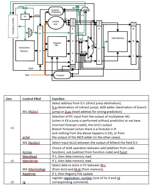
memxcb: xDPU Show how the code is executed in the DPU of the image, as follows:
A Give the single timing diagram resulting from the run, based on the register and memory values listed
above.
B Provide all values generated within the DPU, either as data or control signals, separately for each
machine cycle, from the recall phase of the first instruction, to the result storage phase of the last
instruction.
Step by Step Solution
There are 3 Steps involved in it
1 Expert Approved Answer
Step: 1 Unlock

Question Has Been Solved by an Expert!
Get step-by-step solutions from verified subject matter experts
Step: 2 Unlock
Step: 3 Unlock