

Question: Consider the n-channel E-MOSFET shown below. The process parameters are given as follows: Substrate doping density NA = 2 1015 cm-3 Source/drain doping density
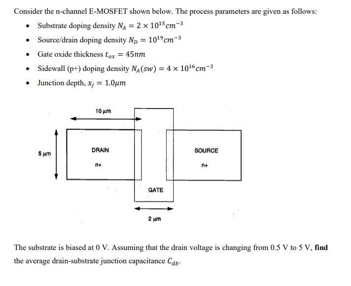
Consider the n-channel E-MOSFET shown below. The process parameters are given as follows: Substrate doping density NA = 2 1015 cm-3 Source/drain doping density N = 1019 cm Gate oxide thickness tox = 45nm -3 Sidewall (p+) doping density NA(sw) = 4 1016 cm Junction depth, xj = 1.0m 5 10m DRAIN n+ GATE SOURCE n+ 2 m The substrate is biased at 0 V. Assuming that the drain voltage is changing from 0.5 V to 5 V, find the average drain-substrate junction capacitance Cdb
Step by Step Solution
There are 3 Steps involved in it
1 Expert Approved Answer
Step: 1 Unlock

Question Has Been Solved by an Expert!
Get step-by-step solutions from verified subject matter experts
Step: 2 Unlock
Step: 3 Unlock