

Question: Using the basic topology of Fig. 8.53, design a CMOS feedback amplifier with R i = , R o < 30 Ω, A v =
Using the basic topology of Fig. 8.53, design a CMOS feedback amplifier with Ri= ˆž, Ro< 30 Ω, Av= Ï…o/Ï…i= 10, and small-signal bandwidth fˆ’3dB> 2 MHz. No peaking is allowed in the gain-versus-frequency response. Supply current must be less than 2 mA from each of ± 5 V supplies. The circuit operates with RL= 1 kΩ to ground and must be able to swing Vo= ± 1 V before clipping occurs. Use the process data of Table 2.1 with Xd= 0.5 µm and γn= 0.5 V1/2. Source and drain regions are 9 µm wide. Verify your hand calculations with SPICE simulations.
Figure 8.53:
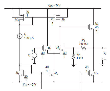
Table 2.1:
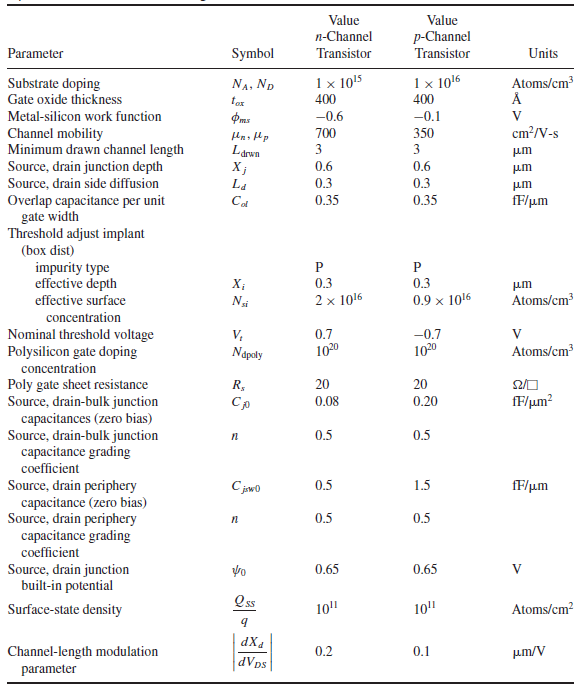
Vpp = 5 V 20 M4 M3 | Mg 1 40 14 100 R4 20 k2 , 40 40 Vo R2 1 k2 40 40 M5 20 M6 M7 Vss =-5 V TRI- -18 Value Value n-Channel p-Channel Parameter Symbol Transistor Transistor Units Substrate doping Gate oxide thickness 1 x 10¹⁵ 1 1016 Atoms/cm NA, ND ter 400 400 Metal-silicon work function Pms -0.6 -0.1 Channel mobility Minimum drawn channel length Source, drain junction depth Source, drain side diffusion Overlap capacitance per unit gate width Threshold adjust implant (box dist) 700 350 cm?/V-s Larwn 3 3 X j 0.6 0.6 um La 0.3 0.3 Cd 0.35 0.35 fF/um impurity type effective depth P X; 0.3 0.3 um effective surface Ni 2 x 10¹⁶ 0.9 x 10¹⁶ Atoms/cm concentration Nominal threshold voltage Polysilicon gate doping concentration V, Napoly 0.7 1020 -0.7 1020 Atoms/cm Poly gate sheet resistance Source, drain-bulk junction capacitances (zero bias) Source, drain-bulk junction capacitance grading R, 20 20 Cp 0.08 0.20 fF/um? 0.5 0.5 coefficient Source, drain periphery capacitance (zero bias) Source, drain periphery capacitance grading C jaw0 0.5 1.5 fF/m 0.5 0.5 coefficient Source, drain junction built-in potential 0.65 0.65 Q ss Surface-state density 10" 10" Atoms/cm? dX4 Channel-length modulation parameter 0.2 0.1 um/V dVps
Step by Step Solution
3.41 Rating (176 Votes )
There are 3 Steps involved in it
V o 1V into R L 1 k need I D8 1 mA Set I D8 2 mA Say 16 mA This lowers R o run m 1 m 2 m 3 at low I ... View full answer

Get step-by-step solutions from verified subject matter experts
Document Format (2 attachments)
1528_605d88e1c5b44_687075.pdf
180 KBs PDF File
1528_605d88e1c5b44_687075.docx
120 KBs Word File