

Question: Consider the sequential circuit implementing serial addition built with two shift registers, a 1 - bit full adder and a D flip - flop (
Consider the sequential circuit implementing serial addition built with two shift registers, a bit full adder and a D flipflop Figure in Morris Mano & Michael Ciletti, Digital Design Design and implement in Verilog a bit version of this circuit. Use the behavioral implementation behavioralserialadder.vl and make the following changesadditions:
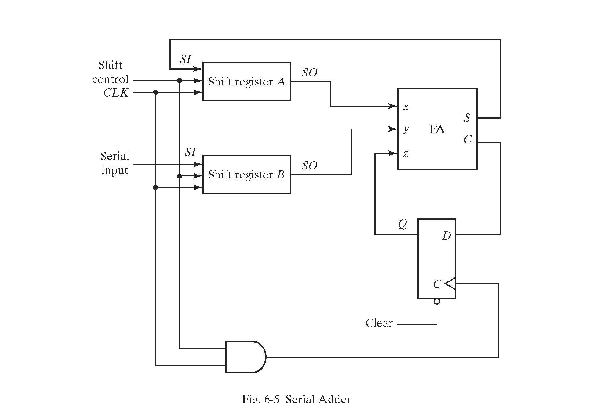
Create a logic diagram of the circuit. Use Figure and update it using the structure of the behavioral model add a x multiplexer and parallel inputs to the shift registers
Cleate a logic diagram of the shift register with parallel load as implemented in module shiftreg block level multiplexers and Dflipflops
Create a state diagram of the serial adder.
Implement modules shiftreg and serialadder at gatelevel using gatelevel Dflipflops, full adder, and x multiplexers
Test the circuit with several inputs adding positive and negative numbers and show the output.
Write a report, including the logic diagrams, the state diagram, the Verilog source code and the test results. Fig is attached here. and behavioralserialadder.vl is below. bit adder using shift registers and bit serial adder
Behavioural model
module adderxySLoad,Clock;
input : xy;
input Load,Clock;
output : S;
wire : PO;
shiftreg rSIxSOSClock,Load
rbySOPOClock,Load;
serialadder saSOSOSIClock,Load;
Uncomment the following line to trace execution
always @negedge Clock $monitorb bSPO;
endmodule
Behavioral shift register with parallel load
Load load;
Load shift
module shiftreg SIPISOPOClock,Load;
input Load,Clock;
input SI; Serial input
input : PI; Parallel input
output SO; Serial output
output : PO; Parallel output
reg : R; Register
assign SO R;
assign PO R;
always @negedge Clock
if Load R PI; Parallel load
else begin Shift right
R R;
R SI;
end
endmodule
Behavioral model of bit serial adder
module serialadderxySClock,Clear;
input xyClock,Clear;
output S;
reg D; simulating D flipflop
wire C;
assign CS xyD; dataflow binary adder
assign C Clear : C; behavioral x multiplexer
always @negedge Clock load D on negative edge
D C;
endmodule
module test;
reg signed : AB;
reg Load, Clock;
wire signed : S;
adder add ABSLoad,Clock;
always # Clock ~Clock; Generate a clock edge at every time unit
initial begin
A; B;
Load; Load inputs and clear the flipflop
Clock; Start Clock
# Load; Start serial adder enable shifing
# $displayd d dABS; Show sum after negaive edges
$finish; Stop clock pulses
end
endmodule
Step by Step Solution
There are 3 Steps involved in it
1 Expert Approved Answer
Step: 1 Unlock

Question Has Been Solved by an Expert!
Get step-by-step solutions from verified subject matter experts
Step: 2 Unlock
Step: 3 Unlock