

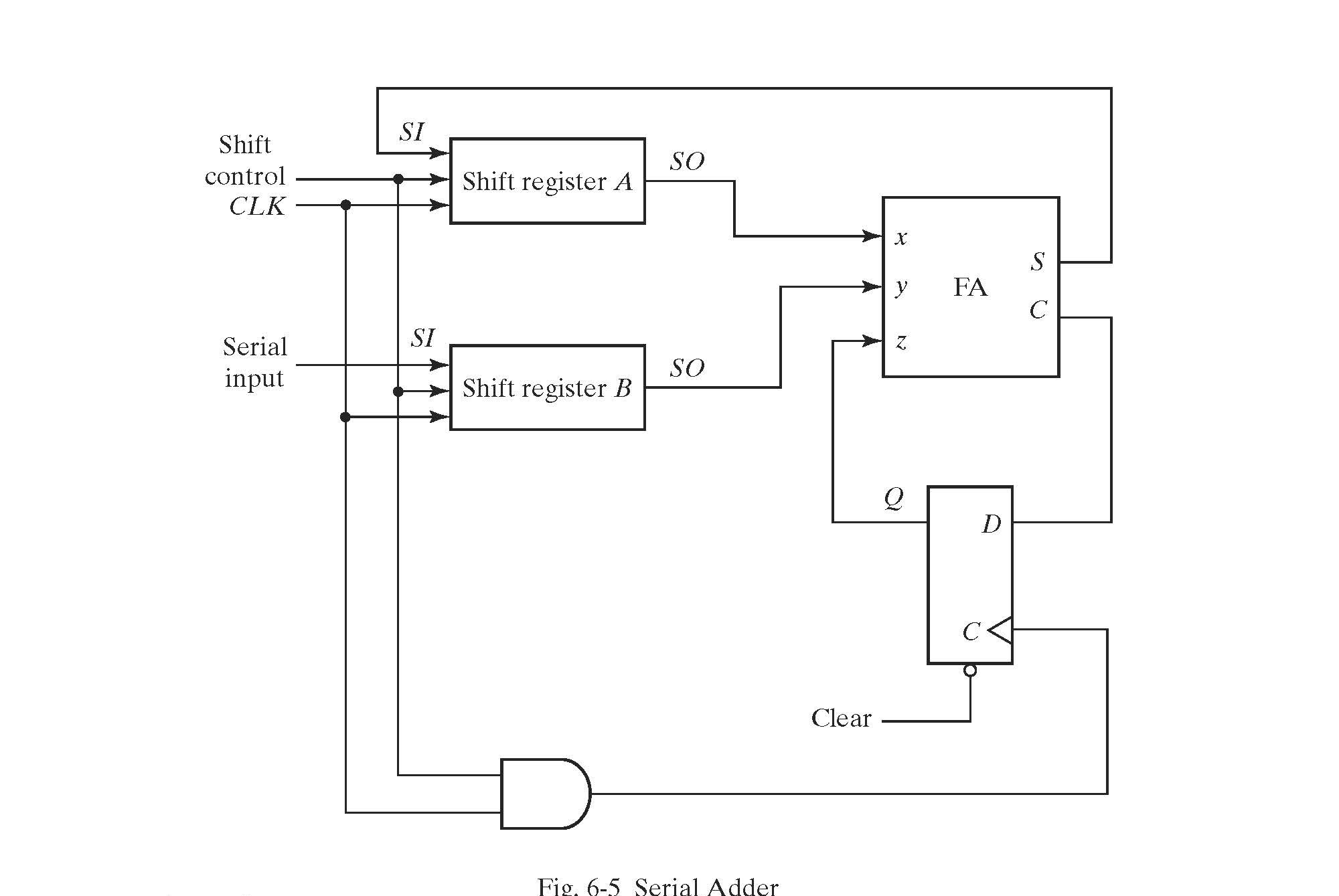
Question: JUST PROVIDE THE VERILOG SOURCE CODE PLEASE. Consider the sequential circuit implementing serial addition built with two shift registers, a 1 - bit full adder
JUST PROVIDE THE VERILOG SOURCE CODE PLEASE. Consider the sequential circuit implementing serial addition built with two shift registers, a bit full adder and a D flipflop Figure Design and implement in Verilog a bit version of this circuit. Use the behavioral implementation behavioralserialadder.vl and make the following changesadditions:
Create a logic diagram of the circuit. Use Figure and update it using the structure of the behavioral model add a x multiplexer and parallel inputs to the shift registers
Cleate a logic diagram of the shift register with parallel load as implemented in module shiftreg block level multiplexers and Dflipflops
Create a state diagram of the serial adder.
Implement modules shiftreg and serialadder at gatelevel using gatelevel Dflipflops, full adder, and x multiplexers.
Test the circuit with several inputs adding positive and negative numbers and show the output.
Write a report, including the logic diagrams, the state diagram, the Verilog source code and the test results. bit adder using shift registers and bit serial adder
Behavioural model
module adderxySLoad,Clock;
input : xy;
input Load,Clock;
output : S;
wire : PO;
shiftreg rSIxSOSClock,Load
rbySOPOClock,Load;
serialadder saSOSOSIClock,Load;
Uncomment the following line to trace execution
always @negedge Clock $monitorb bSPO;
endmodule
Behavioral shift register with parallel load
Load load;
Load shift
module shiftreg SIPISOPOClock,Load;
input Load,Clock;
input SI; Serial input
input : PI; Parallel input
output SO; Serial output
output : PO; Parallel output
reg : R; Register
assign SO R;
assign PO R;
always @negedge Clock
if Load R PI; Parallel load
else begin Shift right
R R;
R SI;
end
endmodule
Behavioral model of bit serial adder
module serialadderxySClock,Clear;
input xyClock,Clear;
output S;
reg D; simulating D flipflop
wire C;
assign CS xyD; dataflow binary adder
assign C Clear : C; behavioral x multiplexer
always @negedge Clock load D on negative edge
D C;
endmodule
module test;
reg signed : AB;
reg Load, Clock;
wire signed : S;
adder add ABSLoad,Clock;
always # Clock ~Clock; Generate a clock edge at every time unit
initial begin
A; B;
Load; Load inputs and clear the flipflop
Clock; Start Clock
# Load; Start serial adder enable shifing
# $displayd d dABS; Show sum after negaive edges
$finish; Stop clock pulses
end
endmoduleHig Serial Adder
Step by Step Solution
There are 3 Steps involved in it
1 Expert Approved Answer
Step: 1 Unlock

Question Has Been Solved by an Expert!
Get step-by-step solutions from verified subject matter experts
Step: 2 Unlock
Step: 3 Unlock