

Question: course:VlsI Design kindly solve given example with full details. Example 6.4 Book (Jan M. Rabey Digital Integrated Circuits 2nd Ed In this example, the intrinsic
course:VlsI Design
kindly solve given example with full details.
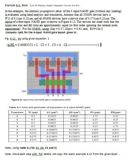
Example 6.4 Book (Jan M. Rabey Digital Integrated Circuits 2nd Ed In this example, the intrinsic propagarion delay of the 4 input NAND gate (without any loading) in evaluated using hand analysis and simulation. Assume that all NMOS devices have a TL of 0.5um/0.25 um, and all PMOS devices have a device size of 0.375um/0.25um. The layout of a four-input NAND gate is shown in Figure 6.12. The devices are sized such that the worst case rise and fall time are approximately equal to first order ignoring the intamal node capacitances). For the MOS. ing. Keg = 0.57, Leger =0.61, and, RN=13k/2 Compute tpHL for the 4-input NAND gate layout given in Fig. 6.12 by using given equation 1 (PHL = 0.69RM C1 +2 - C2+3. C3+4 - CL))- THE Our GND Figure 6.12 Layout a four input NAND gate in complementary CMOS PD) 0.25 025 Table 6.1 Area and perimeter of transistors in 4 input NAND gate Transistor w (m) AS (m) AD (um) PS (m) 05 0.3125 0.0625 1.75 05 0.0625 0.0625 0.25 5 05 0.0625 0.0625 0.25 + 03 00625 0.3125 0.25 5 0.375 0 296875 0.171875 1.875 6 0 375 0 171875 0.171875 0.875 2 0.375 0.171875 0.171875 0875 & 0.375 0 296875 0.171875 1875 0.25 1.75 0.875 0875 0875 0875 Note; Using table 6.1 for C2, C3 and CL Note: Slove each step with full details not copy the exact example 6.12 from the given book
Step by Step Solution
There are 3 Steps involved in it

Get step-by-step solutions from verified subject matter experts