

Question: D Q clock Write a Verilog code to introduce glitch control to the inputs of an adder. The adder receives an additional signal chg that
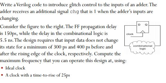
D Q clock Write a Verilog code to introduce glitch control to the inputs of an adder. The adder receives an additional signal chg that is 1 when the adder's inputs are changing Consider the figure to the right. The FF propagation delay is 150ps, while the delay in the combinational logic is 5.5 ns. The design requires that input data does not change its state for a minimum of 300 ps and 400 ps before and after the rising edge of the clock, respectively. Compute the maximum frequency that you can operate this design at, using: Ideal clock A clock with a time-to-rise of 25ps combinational logic D Q clock Write a Verilog code to introduce glitch control to the inputs of an adder. The adder receives an additional signal chg that is 1 when the adder's inputs are changing Consider the figure to the right. The FF propagation delay is 150ps, while the delay in the combinational logic is 5.5 ns. The design requires that input data does not change its state for a minimum of 300 ps and 400 ps before and after the rising edge of the clock, respectively. Compute the maximum frequency that you can operate this design at, using: Ideal clock A clock with a time-to-rise of 25ps combinational logic
Step by Step Solution
There are 3 Steps involved in it

Get step-by-step solutions from verified subject matter experts