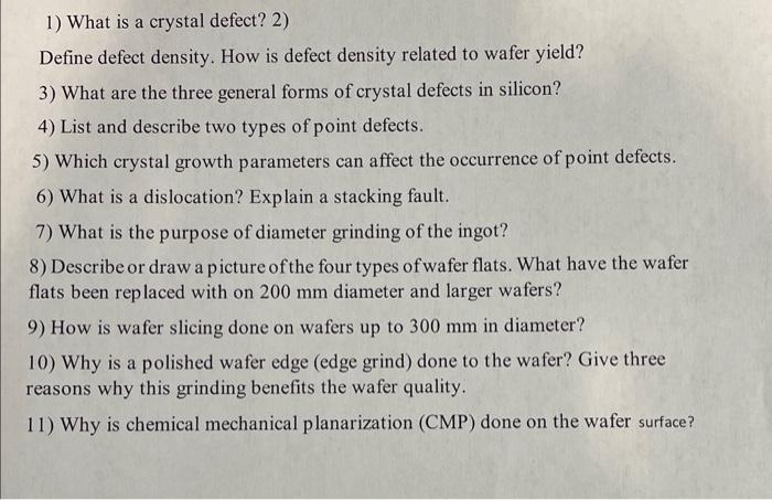
Question: Define defect density. How is defect density related to wafer yield? 3) What are the three general forms of crystal defects in silicon? 4) List

Define defect density. How is defect density related to wafer yield? 3) What are the three general forms of crystal defects in silicon? 4) List and describe two types of point defects. 5) Which crystal growth parameters can affect the occurrence of point defects. 6) What is a dislocation? Explain a stacking fault. 7) What is the purpose of diameter grinding of the ingot? 8) Describe or draw a picture of the four types of wafer flats. What have the wafer flats been replaced with on 200mm diameter and larger wafers? 9) How is wafer slicing done on wafers up to 300mm in diameter? 10) Why is a polished wafer edge (edge grind) done to the wafer? Give three reasons why this grinding benefits the wafer quality. 11) Why is chemical mechanical planarization (CMP) done on the wafer surface
Step by Step Solution
There are 3 Steps involved in it

Get step-by-step solutions from verified subject matter experts


