

Question: Design a 128K x 16 RAM by using a block diagram of RAM chip as shown in Figure 1. Assume that decoder ICs are available
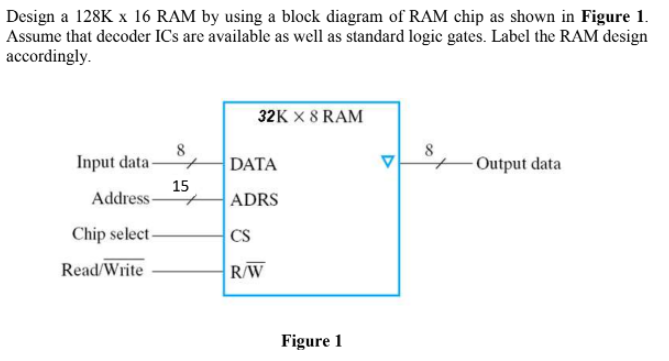
Design a 128K x 16 RAM by using a block diagram of RAM chip as shown in Figure 1. Assume that decoder ICs are available as well as standard logic gates. Label the RAM design accordingly. 32K X 8 RAM 8 Input data DATA Output data 15 Address ADRS Chip select CS Read/Write R/W Figure 1
Step by Step Solution
There are 3 Steps involved in it
1 Expert Approved Answer
Step: 1 Unlock

Question Has Been Solved by an Expert!
Get step-by-step solutions from verified subject matter experts
Step: 2 Unlock
Step: 3 Unlock