

Question: Design a 4 bit adder with the library provided. When does the maximum delay occur? Waveforms as well please. Thank you. ORun Copy Follow the
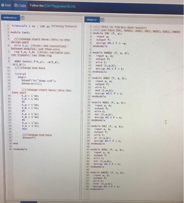
ORun Copy Follow the EDA Playground BLOG 1 timescale 1 ns /100 ps SV/Veriliog Testbench 3 module test; 5 11I/change start here: this is the 1 IIlI this is Tibrary dont touch!! 2 111I you have INV, NAND2, AND2, OR2, NOR2, XOR2, XNOR:2 3 module INV (f, a) 4input a; 5 output f; deisgn part 6 wire ty; I/hint: the connctions 6 assign s0.2 f-a; 7 endmodule between modules, set them wire 7 reg ta, t.b; //hint: variable you 9 module NAND2 (f, a, b)i 10 input a, b; set signals, set them reg 11 output f; 12 wire t; 13 nand (t,a,b) 14 assign #0.3 f-t; 15 endmodule 16 17 module AND2 (f, a, b): 18 input a, b; 19 output f; 20 wire t; 21 and (t,a,b): 22 assign #0.5 f-t; 23 endmodule 24 25 module NOR2 (F. a, b): 26 input a, b; 27 output f 28 wire t; 29 nor (t.a.b): 30 55ign 40.3f-t: 31 endmodule 9 AND2 testnG.fcty), .acta). b(t b)); 10 11//change End here 12 initial 13 begin Sdumpfile("dump. vcd"); 15 16 17 Sdumpvars(): ////change start here: this the t-a 1'bo; test part 18 19 21 25 ta 1'bi; #20 ////change End here 33 module OR2 (f. a, b): 29 30 31 input a, b; 35 output f: 36 wire ti 37 or (t,a,b); 38 assign #0.5 f-t; 9 endmodule Sdumpoff; 34 end 35 36 endmodule 41 module XOR2 (f, a, b) 42 1nput a, b; 43 output f; 44 wire t; 45 xor (t,a,b): 46 assign s0.3f t 47 endnodule 49 module XNOR2 (f, a, b) 50 input a, b 51 output f: 52 wire ti 53 xnor (t,a, b): 54 assign#0.3 fat; 55 endmodule
Step by Step Solution
There are 3 Steps involved in it

Get step-by-step solutions from verified subject matter experts