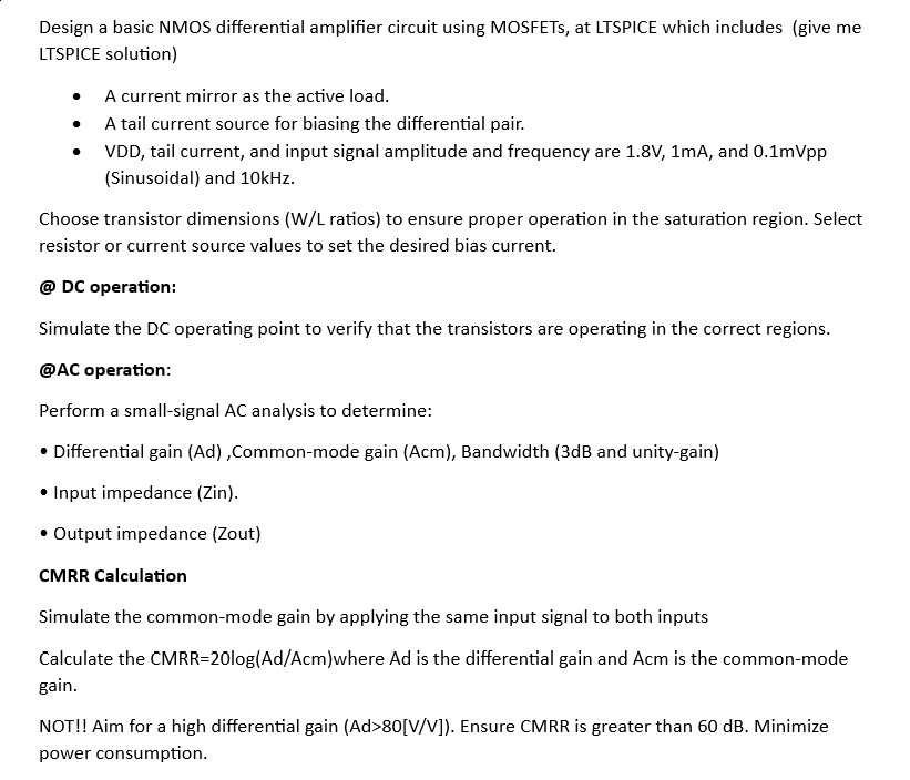
Question: Design a basic NMOS differential amplifier circuit using MOSFETs, at LTSPICE which includes ( give me LTSPICE solution ) - A current mirror as the
Design a basic NMOS differential amplifier circuit using MOSFETs, at LTSPICE which includes give me LTSPICE solution
A current mirror as the active load.
A tail current source for biasing the differential pair.
VDD tail current, and input signal amplitude and frequency are mathrm~Vmathrm~mA and mVpp Sinusoidal and kHz
Choose transistor dimensions WL ratios to ensure proper operation in the saturation region. Select resistor or current source values to set the desired bias current.
@ DC operation:
Simulate the DC operating point to verify that the transistors are operating in the correct regions.
@AC operation:
Perform a smallsignal AC analysis to determine:
Differential gain AdCommonmode gain Acm Bandwidth dB and unitygain
Input impedance Zin
Output impedance Zout
CMRR Calculation
Simulate the commonmode gain by applying the same input signal to both inputs
Calculate the CMRRlogAdAcm where Ad is the differential gain and Acm is the commonmode gain.
NOT!! Aim for a high differential gain AdVV Ensure CMRR is greater than dB Minimize power consumption.

Step by Step Solution
There are 3 Steps involved in it
1 Expert Approved Answer
Step: 1 Unlock


Question Has Been Solved by an Expert!
Get step-by-step solutions from verified subject matter experts
Step: 2 Unlock
Step: 3 Unlock


