Question: Differential Amplifier Design This project requires designing and simulating a differential amplifier using 1 8 0 nm CMOS technology in LTSPICE. The amplifier must include
Differential Amplifier Design
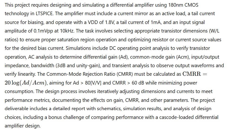
This project requires designing and simulating a differential amplifier using nm CMOS
technology in LTSPICE. The amplifier must include a current mirror as an active load, a tail current
source for biasing, and operate with a VDD of V a tail current of mA and an input signal
amplitude of mVpp at kHz The task involves selecting appropriate transistor dimensions WL
ratios to ensure proper saturation region operation and optimizing resistor or current source values
for the desired bias current. Simulations include DC operating point analysis to verify transistor
operation, AC analysis to determine differential gain Ad commonmode gain Acm inputoutput
impedance, bandwidth dB and unitygain and transient analysis to observe output waveforms and
verify linearity. The CommonMode Rejection Ratio CMRR must be calculated as CMRR
logAdAcm aiming for Ad VV and CMRR dB while minimizing power
consumption. The design process involves iteratively adjusting dimensions and currents to meet
performance metrics, documenting the effects on gain, CMRR and other parameters. The project
deliverable includes a detailed report with schematics, simulation results, and analysis of design
choices, including a bonus challenge of comparing performance with a cascodeloaded differential
amplifier design.

Step by Step Solution
There are 3 Steps involved in it
1 Expert Approved Answer
Step: 1 Unlock


Question Has Been Solved by an Expert!
Get step-by-step solutions from verified subject matter experts
Step: 2 Unlock
Step: 3 Unlock


