

Question: Design a data-flow Verilog module for the following 4-bit BCD adder? Design a combinational circuit for BCD adder. See Figure 4.14 of the textbook for
Design a data-flow Verilog module for the following 4-bit BCD adder?
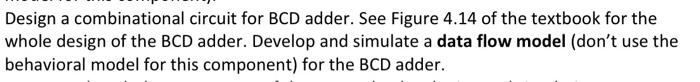
Design a combinational circuit for BCD adder. See Figure 4.14 of the textbook for the whole design of the BCD adder. Develop and simulate a data flow model (don't use the behavioral model for this component) for the BCD adder. Chapter 4 Combinational Logic Addend Augend Carry K out 4-bit binary adder Z8 Z4 Zz Z, Carry in Output carry 0 4-bit binary adder Sg $4 S, S FIGURE 4.14 Block diagram of a BCD adder
Step by Step Solution
There are 3 Steps involved in it
1 Expert Approved Answer
Step: 1 Unlock

Question Has Been Solved by an Expert!
Get step-by-step solutions from verified subject matter experts
Step: 2 Unlock
Step: 3 Unlock