Question: Design an Atmega 2560 microcontroller system which has two chips mapped as external DATA memory. The first chip is an 8Kx8 RAM chip starting at

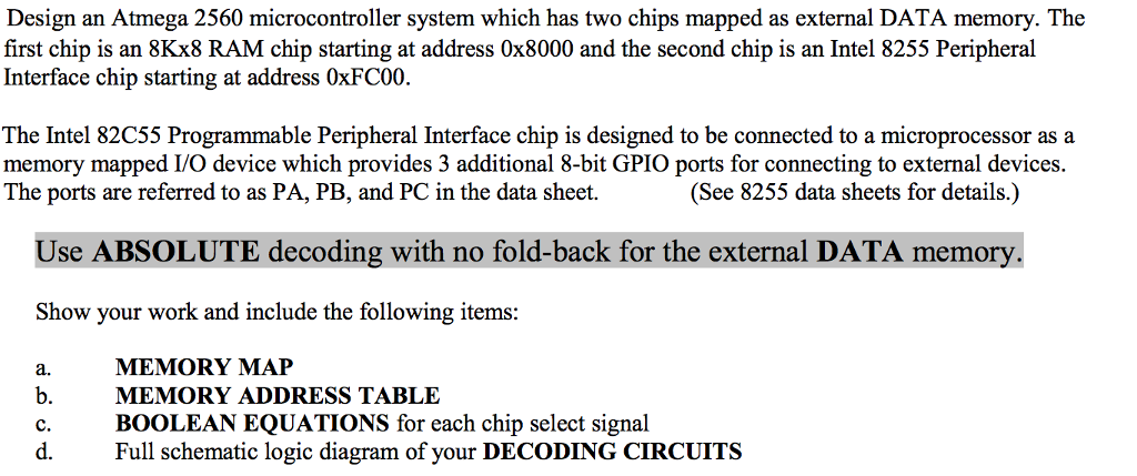
Design an Atmega 2560 microcontroller system which has two chips mapped as external DATA memory. The first chip is an 8Kx8 RAM chip starting at address 0x8000 and the second chip is an Intel 8255 Peripheral Interface chip starting at address 0xFC00 The Intel 82C55 Programmable Peripheral Interface chip is designed to be connected to a microprocessor as a memory mapped Lo device which provides 3 additional 8-bit GPIO ports for connecting to external devices. The ports are referred to as PA, PB, and PC in the data sheet. (See 8255 data sheets for details.) Use ABSOLUTE decoding with no fold-back for the external DATA memory. Show your work and include the following items: MEMORY MAP MEMORY ADDRESS TABLE BOOLEAN EQUATIONS for each chip select signal Full schematic logic diagram of your DECODING CIRCUITS Design an Atmega 2560 microcontroller system which has two chips mapped as external DATA memory. The first chip is an 8Kx8 RAM chip starting at address 0x8000 and the second chip is an Intel 8255 Peripheral Interface chip starting at address 0xFC00 The Intel 82C55 Programmable Peripheral Interface chip is designed to be connected to a microprocessor as a memory mapped Lo device which provides 3 additional 8-bit GPIO ports for connecting to external devices. The ports are referred to as PA, PB, and PC in the data sheet. (See 8255 data sheets for details.) Use ABSOLUTE decoding with no fold-back for the external DATA memory. Show your work and include the following items: MEMORY MAP MEMORY ADDRESS TABLE BOOLEAN EQUATIONS for each chip select signal Full schematic logic diagram of your DECODING CIRCUITS
Step by Step Solution
There are 3 Steps involved in it

Get step-by-step solutions from verified subject matter experts


