

Question: Design and simulate a combinational circuit Using Quartus II simulator. Your design must read 4-bit BCD and convert it to 5211 number system. The input
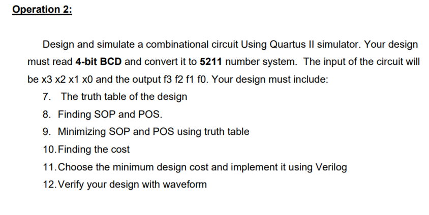 Design and simulate a combinational circuit Using Quartus II simulator. Your design must read 4-bit BCD and convert it to 5211 number system. The input of the circuit will be x3 x2 x1 x0 and the output f3 f2 f1 f0. Your design must include: 7. The truth table of the design 8. Finding SOP and POS. 9. Minimizing SOP and POS using truth table 10.Finding the cost 11.Choose the minimum design cost and implement it using Verilog 12.Verify your design with waveform
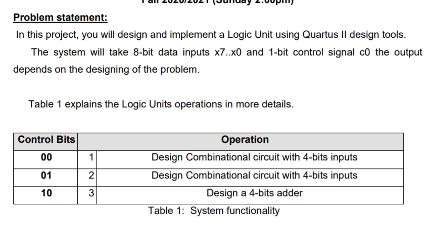
Problem statement: In this project, you will design and implement a Logic Unit using Quartus II design tools. The system will take 8-bit data inputs x7..x0 and 1-bit control signal co the output depends on the designing of the problem. Table 1 explains the Logic Units operations in more details. Control Bits 00 1 01 2 Operation Design Combinational circuit with 4-bits inputs Design Combinational circuit with 4-bits inputs Design a 4-bits adder Table 1: System functionality 10 3 Operation 2: Design and simulate a combinational circuit Using Quartus Il simulator. Your design must read 4-bit BCD and convert it to 5211 number system. The input of the circuit will be x3 x2 x1 x0 and the output f3 f2 f1 fo. Your design must include: 7. The truth table of the design 8. Finding SOP and POS. 9. Minimizing SOP and POS using truth table 10.Finding the cost 11. Choose the minimum design cost and implement it using Verilog 12. Verify your design with waveform
Step by Step Solution
There are 3 Steps involved in it

Get step-by-step solutions from verified subject matter experts