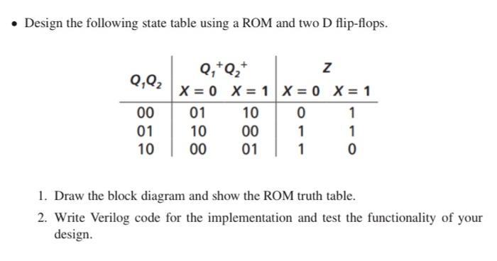
Question: Design the following state table using a ROM and two D flip-flops. Q,02 00 01 10 Q+Q+ Z X=0 X = 1| X=0 X

Design the following state table using a ROM and two D flip-flops. Q,02 00 01 10 Q+Q+ Z X=0 X = 1| X=0 X = 1 01 10 0 1 10 00 1 1 00 01 1 0 1. Draw the block diagram and show the ROM truth table. 2. Write Verilog code for the implementation and test the functionality of your design.
Step by Step Solution
3.32 Rating (155 Votes )
There are 3 Steps involved in it
From Given Data a Construct truth table for the sequential circuit is as shown ... View full answer

Get step-by-step solutions from verified subject matter experts


