

Question: Digital logic design lab Q1. Design a circuit detect sequence: 110. Q2. Design an odd counter using JK flip flop. Q3. Complete the following timing
Digital logic design lab 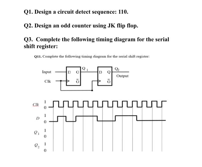
Q1. Design a circuit detect sequence: 110. Q2. Design an odd counter using JK flip flop. Q3. Complete the following timing diagram for the serial shift register: Q11. Complete the following timing diagram for the serial shift register: Input DO D Output Cik 7 CIK mre D 0 1 2, 0
Step by Step Solution
There are 3 Steps involved in it
1 Expert Approved Answer
Step: 1 Unlock

Question Has Been Solved by an Expert!
Get step-by-step solutions from verified subject matter experts
Step: 2 Unlock
Step: 3 Unlock