

Question: f . With input of Q 1 = logic 1 ( VoD ) , record the result for each: ( 3 ) If input to
f With input of logicVoD record the result for each:
If input to QDG logic output PR
If input to QDG logic output PR
Based on the results, what type of logic gate does this circuit represent?
a AND
b
c NAND
d NOR
Part
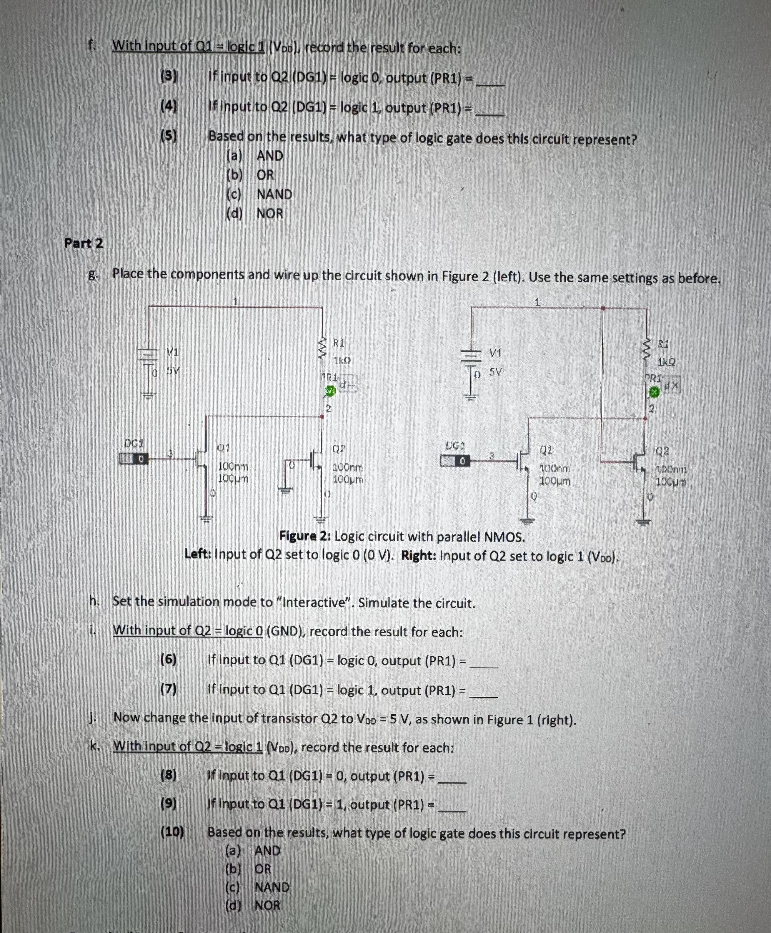
g Place the components and wire up the circuit shown in Figure left Use the same settings as before.
rigure : Logc circuit with parallel NMOS.
Left: Input of Q set to logic V Right: Input of Q set to logic Voo
h Set the simulation mode to "Interactive". Simulate the circuit.
i With input of logicGND record the result for each:
If input to QDG logic output PR
If input to QDG logic output PR
j Now change the input of transistor to as shown in Figure right
k With input of logic record the result for each:
If input to QDG output PR
If input to QDG output PR
Based on the results, what type of logic gate does this circuit represent?
a AND
b
c NAND
d NOR
THIS IS PAGE TO A PREVIOUS POST, I COULDNT FIGURE OUT HOW TO SEND THEM TOGETHER
Step by Step Solution
There are 3 Steps involved in it
1 Expert Approved Answer
Step: 1 Unlock

Question Has Been Solved by an Expert!
Get step-by-step solutions from verified subject matter experts
Step: 2 Unlock
Step: 3 Unlock