

Question: For this assignment, you will design and simulate a simplified ARM single-cycle processor using SystemVerilog. You will combine your ALU from Assignment #2 with the
For this assignment, you will design and simulate a simplified ARM single-cycle processor using SystemVerilog. You will combine your ALU from Assignment #2 with the code for the rest of the processor taken from our textbook. Then you will load a test program and confirm that the system works. Next, you will implement two new instructions, and then write a new test program that confirms the new instructions work as well. By the end of this assignment, you should thoroughly understand the internal operation of the ARM single-cycle processor.
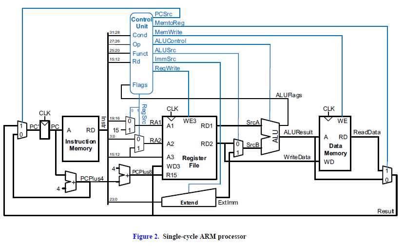
The details of the simplified ARM single-cycle processor are given in Section 7.3 of our text. The single-cycle processor schematic from the text is repeated at the end of this assignment for your convenience. This version of the ARM single-cycle processor can execute the following instructions: ADD, SUB, AND, ORR, LDR, STR, and B.
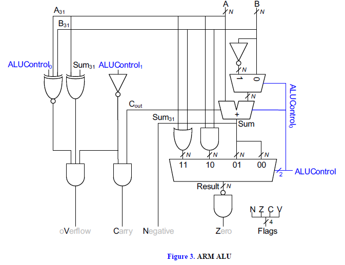
Our model of the single-cycle ARM processor divides the machine into two major units: the control and the datapath. Each unit is constructed from various functional blocks. For example, as shown in the figure on the last page of this lab, the datapath contains the 32-bit ALU that you designed in Assignment #2, the register file, the sign extension logic, and five multiplexers to choose appropriate operands.
1. ARM Single-Cycle Processor
The SystemVerilog single-cycle ARM module is given in Section 7.6 of the text. Use the electronic versions of all these files provided on the textbook website.
Study the files until you are familiar with their contents. Look in arm.sv. The top-level module (named top) contains the arm processor (arm) and the data and instruction memories (dmem and imem). Now look at the processor module (called arm). It instantiates two sub-modules, controller and datapath. Now take a look at the controller module and its submodules. It contains two sub-modules: decode and condlogic. The decode module produces all but three control signals. The condlogic module produces those remaining three control signals that update architectural state (RegWrite, MemWrite) or determine the next PC (PCSrc). These three signals depend on the condition mnemonic from the instruction (Cond3:0) and the stored condition flags (Flags3:0) that are internal to the condlogic module. The condition flags produced by the ALU (ALUFlags3:0) are updated in the flags registers dependent on the S bit (FlagW1:0) and on whether the instruction is executed (again, dependent on the condition mnemonic Cond3:0 and the stored value of the condition flags Flags3:0). Make sure you thoroughly understand the controller module. Correlate signal names in the SystemVerilog code with the wires on the schematic.
After you thoroughly understand the controller module, take a look at the datapath SystemVerilog module. The datapath has quite a few submodules. Make sure you understand why each submodule is there and where each is located on the ARM single-cycle processor schematic. Youll notice that the alu module is not defined. Be sure the module name matches the instance module name (alu), and make sure the inputs and outputs are in the same order as in they are expected in the datapath module.
The instruction and data memories instantiated in the top module are each a 64-word 32-bit array. The instruction memory needs to contain some initial values representing the program. The test program is given in Figure 7.60. Study the program until you understand what it does. The machine language code for the program is stored in memfile.dat.
2. Testing the single-cycle ARM processor
In a complex system, if you dont know what to expect the answer should be, you are unlikely to get the right answer. Begin by predicting what should happen on each cycle when running the program. Complete the chart in Table 1 at the end of the lab with your predictions. What address will the final STR instruction write to and what value will it write?
Simulate your processor with ModelSim. Be sure to add all of the .sv files, including the one containing your ALU. Add all of the signals from Table 1 to your waves window. (Note that many are not at the top level; youll have to drill down into the appropriate part of the hierarchy to find them.)
Run the simulation. If all goes well, the testbench will print Simulation succeeded. Look at the waveforms and check that they match your predictions in Table 1. If they dont, the problem is likely in your ALU or because you didnt properly add all of the files.
If you need to debug, youll likely want to view more internal signals. However, on the final waveform that you turn in, show ONLY the following signals in this order: clk, reset, PC, Instr, ALUResult, WriteData, MemWrite, and ReadData. All the values need to be output in hexadecimal and must be readable to get full credit.
After you have fixed any bugs, print out your final waveform.
3. Modifying the ARM single-cycle processor
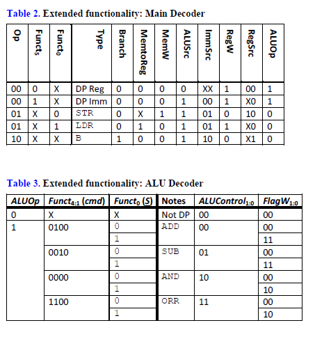
You now need to modify the ARM single-cycle processor by adding the EOR and LDRB instructions. First, modify the ARM processor schematic/ALU at the end of this lab to show what changes are necessary. You can draw your changes directly onto the schematics. Then modify the main decoder and ALU decoder as required. Show your changes in the tables at the end of the lab. Finally, modify the SystemVerilog code as needed to include your modifications.
4. Testing your modified ARM single-cycle processor
Next, youll need a test program to verify that your modified processor works. The program should check that your new instructions work properly and that the old ones didnt break. Use memfile2.asm below.
MAIN SUB R0, R15, R15 ADD R1, R0, #255
ADD R2, R1, R1
STR R2, [R0, #196]
EOR R3, R1, #77
AND R4, R3, #0x1F
ADD R5, R3, R4
LDRB R6, [R5] LDRB R7, [R5, #1]
SUBS R0, R6, R7
BLT MAIN BGT HERE STR R1, [R4, #110]
B MAIN HERE STR R6, [R4, #110]
Convert the program to machine language and put it in a file named memfile2.dat. Modify imem to load this file. Modify the testbench to check for the appropriate address and data value indicating that the simulation succeeded. Run the program and check your results. Debug if necessary. When you are done, print out the waveforms as before and indicate the address and data value written by the final STR instruction.
Must be done in SystemVerilog
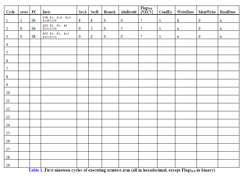
Flags3:0 Cycle reset PC Instr Src SrcB Branch AluResult NZCVI CondEx WriteData MemWrite ReadData Table 1. First nineteen cycles of executing armtest.asm (all in hexadecimal, except Flags3.0 in binary Flags3:0 Cycle reset PC Instr Src SrcB Branch AluResult NZCVI CondEx WriteData MemWrite ReadData Table 1. First nineteen cycles of executing armtest.asm (all in hexadecimal, except Flags3.0 in binary
Step by Step Solution
There are 3 Steps involved in it

Get step-by-step solutions from verified subject matter experts