

Question: Figure 1 : Schematic of single - cycle MIPS processor Our model of the single - cycle MIPS processor divides the machine into two major
Figure : Schematic of singlecycle MIPS processor
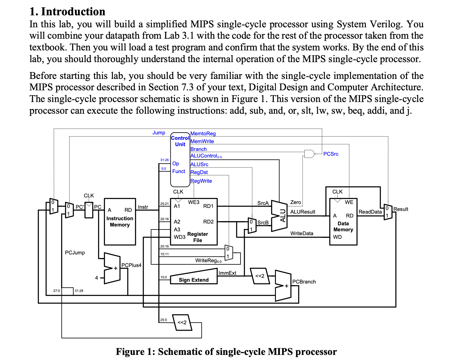
Our model of the singlecycle MIPS processor divides the machine into two major units: the control and the datapath. Each unit is constructed from various functional blocks. For example,
as shown in the Figure the datapath contains the bit ALU that you designed in Lab the register file, the sign extension logic, and five multiplexers to choose appropriate operands.
MIPS SingleCycle Processor
The SystemVerilog singlecycle MIPS module is given in Section of the text. Digital version LabsvCode.rar of the modules will also be uploaded on LMS Study the modules until you are familiar with their contents. Look at the mips module, which instantiates two submodules, controller and datapath. Then take a look at the controller module and its submodules. It contains two submodules: maindec and aludec. The maindec module produces all control signals except those for the ALU. The aludec module produces the control signal, alucontrol : for the ALU. Make sure you thoroughly understand the controller module. Correlate signal names in the System Verilog code with the wires on the schematic.
After you thoroughly understand the controller module, take a look at the datapath System Verilog module. The datapath has quite a few submodules. Make sure you understand why each submodule is there and where each is located on the MIPS singlecycle processor schematic. You'll notice that the alu module is not defined. Include your alu module from Lab into processor. Be sure the module name matches the instance module name alu and make sure the inputs and outputs are in the same order as in they are expected in the datapath module.
The highestlevel module, top, includes the instruction and data memories as well as the processors. Each of the memories is a word times bit array. The instruction memory needs to contain some initial values representing the program. The test program is given in Figure of the textbook. Study the program until you understand what it does. Copy the machine language code for the program and stored it in hexfile.dat. Testing the singlecycle MIPS processor
In this section, you will test the processor you have designed. Simulate your processor with EDA Playground. Be sure to add all of the sv files, including the one containing your ALU. Also add the file hexfile.dat to the test bench as shown in Figure
Figure : Adding hexfile.dat to the test bench Now run the test bench as given below also included in LabsvCode.rar:
Testbench for MIPS processor
saiful.islam@tedu.edu.tr Nov
module testbench;
logic clk;
logic reset;
logic : writedata, dataadr;
logic memwrite;
int correctdata ;
instantiate device to be tested
top dutclk reset, writedata, dataadr, memwrite;
initialize test
initial
begin
reset ; # ; reset ;
end
generate clock to sequence tests
always
begin
clk ; # ; clk ; # ;
end
check that gets written to address
always@negedge clk
begin
ifmemwrite & dataadr begin
$display;
$displayData Address: d Correct data: d dataadr, correctdata;
ifwritedata correctdata begin
$displaySimulation succeeded: ;
$displayData Address: d Data written: d dataadr, writedata;
$display;
$stop;
end else if dataadr writedata correctdata begin
$displaySimulation failed";
$displayData Address: d Data written: d dataadr, writedata;
$display;
$stop;
end
end
end
endmodule
Read the program carefully and note that final sw instruction will write to the address So if all goes well, the testbench will print "Simulation succeeded." If not, the problem is likely in your ALU or because you didn't properly add all of the files. In this case, you need to recheck that all the modules are added correctly. Assignment
Design the MIPS single cycle processor that supports the following instructions: addi, add, sub, and, or slt lw sw beq, and j
Write your own test program other than the example program given in the textbook. Convert is in machine code and change the hexfile.dat. The following table could be used to compute the bit machine instructions for the program.
Step by Step Solution
There are 3 Steps involved in it
1 Expert Approved Answer
Step: 1 Unlock

Question Has Been Solved by an Expert!
Get step-by-step solutions from verified subject matter experts
Step: 2 Unlock
Step: 3 Unlock