

Question: Given the circuit shown in the following figure, and based on the 180 nm TSMC Technology, assume that the supply voltage (VDD) is 1.8V,
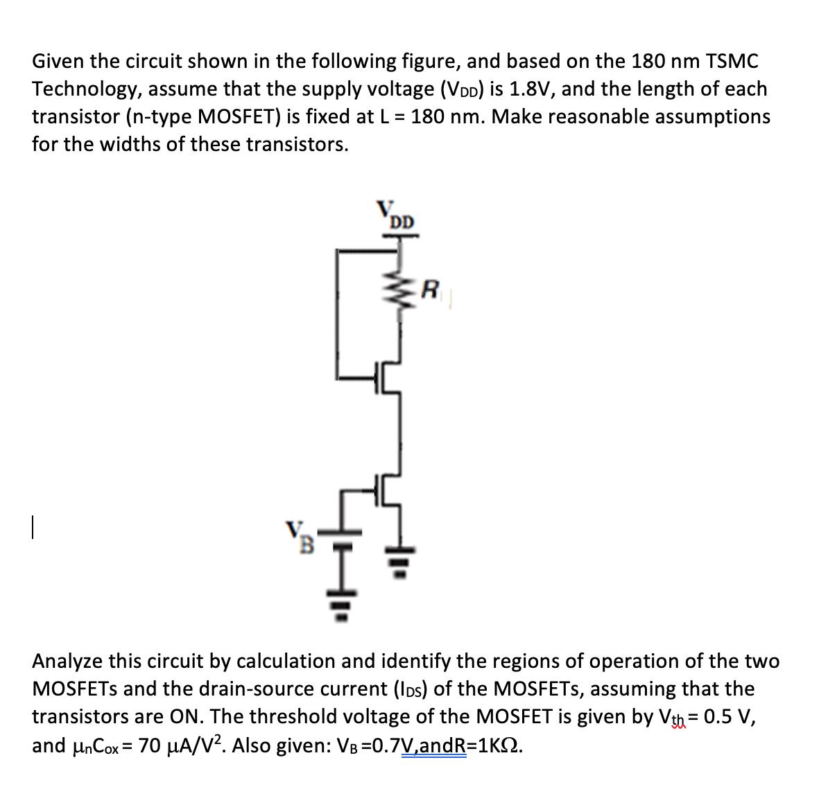
Given the circuit shown in the following figure, and based on the 180 nm TSMC Technology, assume that the supply voltage (VDD) is 1.8V, and the length of each transistor (n-type MOSFET) is fixed at L = 180 nm. Make reasonable assumptions for the widths of these transistors. V DD R Analyze this circuit by calculation and identify the regions of operation of the two MOSFETs and the drain-source current (IDS) of the MOSFETs, assuming that the transistors are ON. The threshold voltage of the MOSFET is given by Vth = 0.5 V, and nCox = 70 A/V. Also given: VB =0.7V, and R=1KQ.
Step by Step Solution
There are 3 Steps involved in it
The given circuit is a CMOS inverter with a pullup resistor which is not a typical CMOS design but its used for learning purposes In this circuit we h... View full answer

Get step-by-step solutions from verified subject matter experts