

Question: helpp III. Figure below shows a simplifled timing diagram for a DRAM read operation over a bus. The access time is considered to last from
helpp
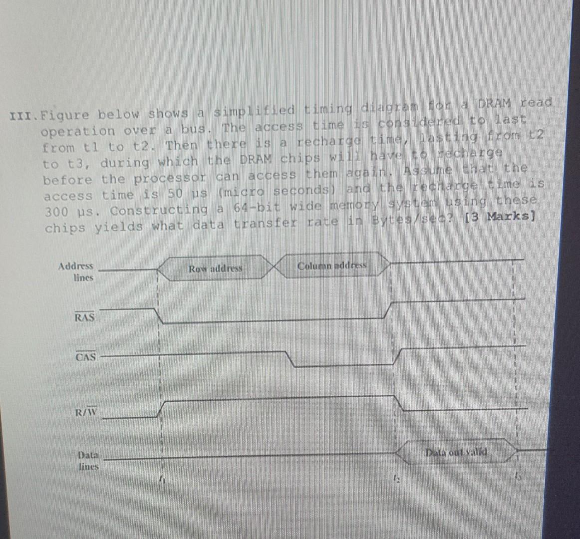
III. Figure below shows a simplifled timing diagram for a DRAM read operation over a bus. The access time is considered to last from t1 to t2. Then there is a recharge time, lasting from t2 to t3, during which the DRAM chips will have to recharge before the processor can access them again. Assume that the access time is 50s (micro seconds) and the rechange time is 300 Hs. Constructing a 64-bit wide memory system using these chips yields what data transfer rate in Bytes/sec? [3 Marks]
Step by Step Solution
There are 3 Steps involved in it
1 Expert Approved Answer
Step: 1 Unlock

Question Has Been Solved by an Expert!
Get step-by-step solutions from verified subject matter experts
Step: 2 Unlock
Step: 3 Unlock