

Question: I need help getting started on the lay out. I am questionable about how the memory controller will look (what will the array look like?
|
I need help getting started on the lay out. I am questionable about how the memory controller will look (what will the array look like? Homework 1 Computer Systems | |
| Instructions | |
| Based on Fig. 6.3, design/draw the layout of a memory module in Fig. 6.5 Note: the memory capacity of Fig. 6.3 is 128 bit(16-byte), each DRAM memory capacity in Fig. 6.5 is 8 Mega-byte.
| |
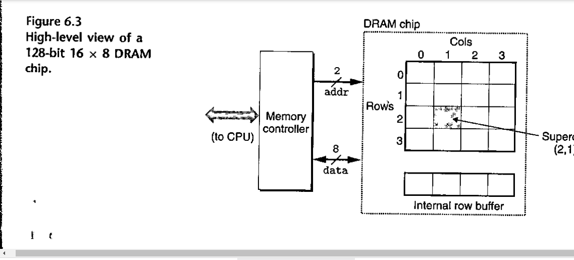
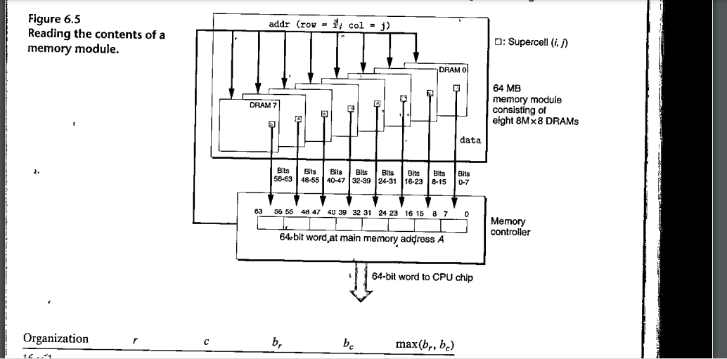
DRAM chip Figure 6.3 High-level view of a 128-bit 16 x 8 DRAM chip. Cols 1 2 0 3 2 0 addr 1 Row's 2 Memory controller (to CPU) 3 Superc (2,1 8 data Internal row buffer addr (row = 1; col = j) Figure 6.5 Reading the contents of a memory module. O: Supercell (1,7) DRAM O DRAM 7 64 MB memory module consisting of eight 8MX 8 DRAMS data Bits 56-69 Bits Bits Bits Bits Bits Bits 48-5540-4732-39 24-31 16-23 8-15 Bits 0-7 63 56 55 48 47 40 39 32 31 24 23 16 15 8 7 o Memory controller 64-bit word at main memory address A 64-bit word to CPU chip Organization b, bc max(br, bc) DRAM chip Figure 6.3 High-level view of a 128-bit 16 x 8 DRAM chip. Cols 1 2 0 3 2 0 addr 1 Row's 2 Memory controller (to CPU) 3 Superc (2,1 8 data Internal row buffer addr (row = 1; col = j) Figure 6.5 Reading the contents of a memory module. O: Supercell (1,7) DRAM O DRAM 7 64 MB memory module consisting of eight 8MX 8 DRAMS data Bits 56-69 Bits Bits Bits Bits Bits Bits 48-5540-4732-39 24-31 16-23 8-15 Bits 0-7 63 56 55 48 47 40 39 32 31 24 23 16 15 8 7 o Memory controller 64-bit word at main memory address A 64-bit word to CPU chip Organization b, bc max(br, bc)
Step by Step Solution
There are 3 Steps involved in it

Get step-by-step solutions from verified subject matter experts