

Question: Implement the Full Adder circuit shown on slide 14. Show the Logisim version (picture) of the circuit and its corresponding Truth table. ADDER Designed to
Implement the Full Adder circuit shown on slide 14. Show the Logisim version (picture) of the circuit and its corresponding Truth table.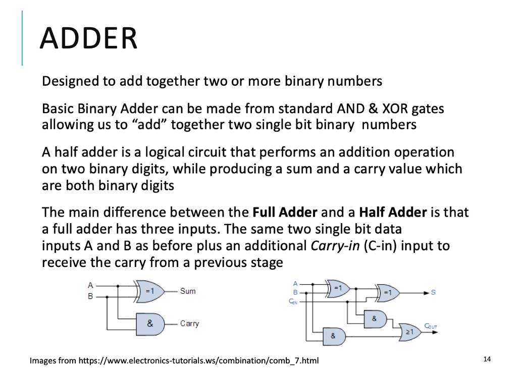
ADDER Designed to add together two or more binary numbers Basic Binary Adder can be made from standard AND & XOR gates allowing us to "add" together two single bit binary numbers A half adder is a logical circuit that performs an addition operation on two binary digits, while producing a sum and a carry value which are both binary digits The main difference between the Full Adder and a Half Adder is that a full adder has three inputs. The same two single bit data inputs A and B as before plus an additional Carry-in (C-in) input to receive the carry from a previous stage -1 Sum 8 GN &Carry COUT Images from https://www.electronics-tutorials.ws/combination/comb_7.html 14
Step by Step Solution
There are 3 Steps involved in it

Get step-by-step solutions from verified subject matter experts