

Question: In Quartus prime block diagram, Design a 4 bit shift L/R shift register using 4-1 mux that would match following tb result. Just provide block
In Quartus prime block diagram, Design a 4 bit shift L/R shift register using 4-1 mux that would match following tb result. Just provide block diagram no other components necessary 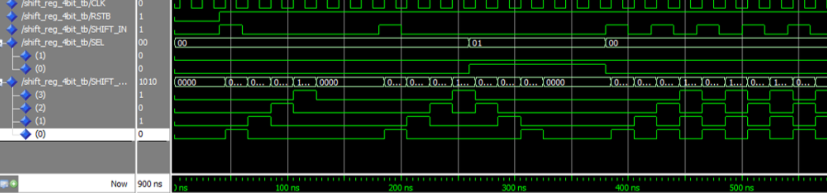
V. C IL 100 101 100 /shift_reg_4bit_tb/CLK /shift_reg_4bit_tb/RSTB 1 /shift_reg_4bit_tb/SHIFT_IN 1 /shift_reg_4bit_tb/SEL 00 (1) 10 (0) 0 /shift_reg_4bit_tb/SHIFT_.... 1010 (3) 1 (2) 10 1 (0) 0 0000 0...0...0...1...0000 10...0...0........0...0...0... 0000 0...0...0... 1...0... 1...1 0... 1...0... Now 900 ns ns 100 ns 200 ns 300 ns 400 ns 500 ns
Step by Step Solution
There are 3 Steps involved in it
1 Expert Approved Answer
Step: 1 Unlock

Question Has Been Solved by an Expert!
Get step-by-step solutions from verified subject matter experts
Step: 2 Unlock
Step: 3 Unlock