

Question: Instructions: Using 1.3 and 1.4 show the program executing for the following program: Figure 1.3 Consider a simple example using a hypothetical processor that includes
Instructions: Using 1.3 and 1.4 show the program executing for the following program:
Figure 1.3
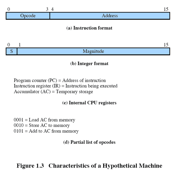
Consider a simple example using a hypothetical processor that includes the characteristics listed in Figure 1.3 . The processor contains a single data register, called the accumulator (AC). Both instructions and data are 16 bits long, and memory is organized as a sequence of 16-bit words. The instruction format provides 4 bits for the opcode, allowing as many as 24 =16 different opcodes (represented by a single hexadecimal digit). The opcode defines the operation the processor is to perform. With the remaining 12 bits of the instruction format, up to 212 =4,096 (4K) words of memory (denoted by three hexadecimal digits) can be directly addressed.
Figure 1.4
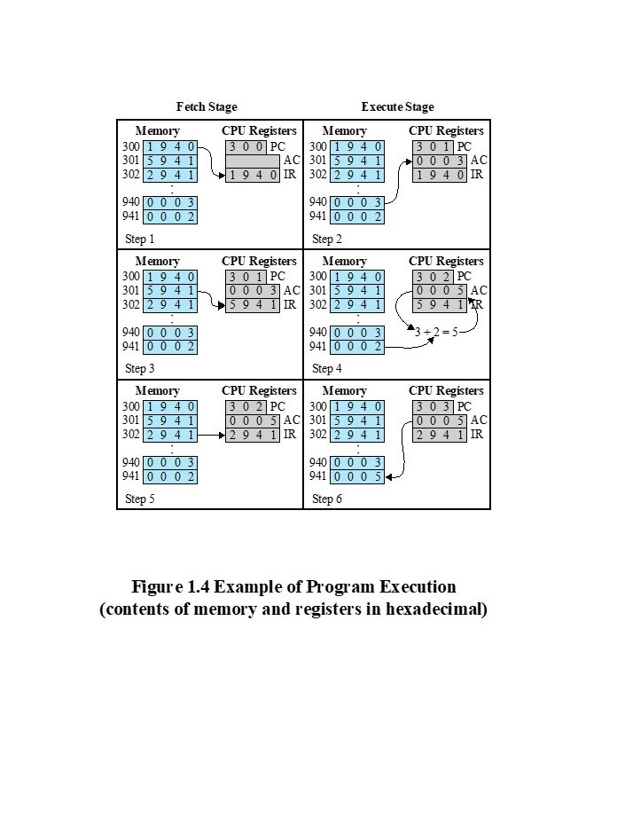 Figure 1.4 illustrates a partial program execution, showing the relevant portions of memory and processor registers. The program fragment shown adds the contents of the memory word at address 940 to the contents of the memory word at address 941 and stores the result in the latter location. Three instructions, which can be described as three fetch and three execute stages, are required:
1. The PC contains 300, the address of the first instruction. The instruction (the value 1940 in hexadecimal) is loaded into the IR and the PC is incremented. Note that this process involves the use of a memory address register (MAR) and a memory buffer register (MBR). For simplicity, these intermediate registers are not shown.
2. The first 4 bits (first hexadecimal digit) in the IR indicate that the AC is to be loaded from memory. The remaining 12 bits (three hexadecimal digits) specify the address, which is 940.
3. The next instruction (5941) is fetched from location 301 and the PC is incremented.
4. The old contents of the AC and the contents of location 941 are added and the result is stored in the AC.
5. The next instruction (2941) is fetched from location 302 and the PC is incremented.
6. The contents of the AC are stored in location 941.
In this example, three instruction cycles, each consisting of a fetch stage and an execute stage, are needed to add the contents of location 940 to the contents of 941. With a more complex set of instructions, fewer instruction cycles would be needed. Most modern processors include instructions that contain more than one address. Thus the execution stage for a particular instruction may involve more than one reference to memory. Also, instead of memory references, an instruction may specify an I/O operation.
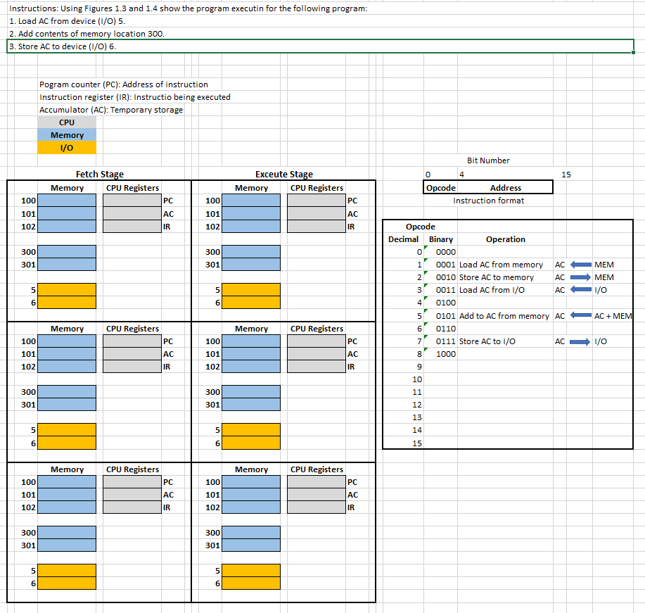
Instructions: Using 1.3 and 1.4 show the program executing for the following program:
1. Load AC from device (I/)) 5.
2. Add contents of memory location 300.
3. Store AC to device (I/0) 6.
0 34 15 Opcode Address (a) Instruction format 15 0 1 S Magnitude (b) Integer format Program counter (PC) = Address of instruction Instruction register (IR) = Instruction being executed Accumulator (AC) = Temporary storage (c) Internal CPU registers 0001 = Load AC from memory 0010 = Store AC to memory 0101 = Add to AC from memory (d) Partial list of opcodes Figure 1.3 Characteristics of a Hypothetical Machine Fetch Stage Execute Stage Memory CPU Register's Memory CPU Registers 300 1 9 40 30 OPC 300 1 9 4 0 3 0 1 PC 301 5 9 4 1 AC 301 5 9 4 1 000 3 AC 3022 9 41 1 9 4 O IR 3022 94 1 1 9 4 0 IR 940 0 0 0 3 941 0 0 0 2 Step 1 Memory 300 1 9 4 0 301 5 9 41 3022 9 4 1 940 0 0 0 3 941 0 0 0 2 Step 2 CPU Registers Memory 30 1 PC 300 1 9 4 01 0 0 0 3 AC 301 5 9 4 1 59 4 1 IR 302 2 9 4 1 CPU Register's 3 0 2 PC 0 0 0 3 ACI 59 4 1 R 23+2 = 5- 940 0 0 0 3 941 0 0 0 2 Step 3 Memory 300 1 9 40 301 5 9 4 1 3022 9 4 1 940 0 0 0 3 941 0 0 0 2 Step 4 CPU Register's Memory 3 0 2 PC 3001 940 0 0 0 5 AC 301 5 9 4 1 2 9 4 1 IR 302 2 9 4 1 CPU Register's 3 0 3 PC 0 0 0 SACI 2 9 4 1 IR 940 0 0 0 3 941 0 0 0 2 Step 5 940 0 0 0 3 941 0 0 0 5 Step 6 Figure 1.4 Example of Program Execution (contents of memory and registers in hexadecimal) Instructions: Using Figures 1.3 and 1.4 show the program executin for the following program: 1. Load AC from device (1/0) 5. 2. Add contents of memory location 300. 3. Store AC to device (1/0) 6. Pogram counter (PC): Address of instruction Instruction register (IR): Instructio being executed Accumulator (AC): Temporary storage CPU Memory 1/0 Bit Number 15 Fetch Stage Memory CPU Registers PC Exceute Stage Memory CPU Registers PC 0 4 Opcode Address Instruction format 100 100 101 AC 101 102 AC IR 102 IR 300 301 300 301 MEM MEM 1/0 5 5 6 6 Opcode Decimal Binary Operation 0 0000 1 0001 Load AC from memory AC 2 0010 Store AC to memory AC 3 0011 Load AC from 1/0 AC 4 0100 5 0101 Add to AC from memory AC 6 0110 7 0111 Store AC to 1/0 AC 8 1000 9 10 AC + MEM Memory Memory 100 CPU Registers PC AC 100 CPU Registers PC AC 1/0 101 101 102 IR 102 IR 300 301 300 301 11 12 13 5 5 14 6 6 15 Memory Memory CPU Registers PC CPU Registers PC 100 101 AC 100 101 102 AC 102 IR IR 300 301 300 301 5 5 6 6
Step by Step Solution
There are 3 Steps involved in it

Get step-by-step solutions from verified subject matter experts