

Question: Logic Circuit Design Procedure 1 ) Determine and assign a letter to the inputs and outputs of the circuit 2 ) Make a truth table
Logic Circuit Design Procedure
Determine and assign a letter to the inputs and outputs of the circuit
Make a truth table
Simplify the stated problem using Kmap method
Draw the logic diagram of the circuit
Simulate the logic circuit
a Combinational Circuit Design I
Design a combinational circuit with four inputs A B C D and one output F Suppose that F is equal to when A and B or A and C or A and D otherwise the output is to be equal to
i Write the truth table and design the circuit of the simplified F function with NAND gates only. PDF
ii Draw the Logic Diagram of the circuit. Proteus
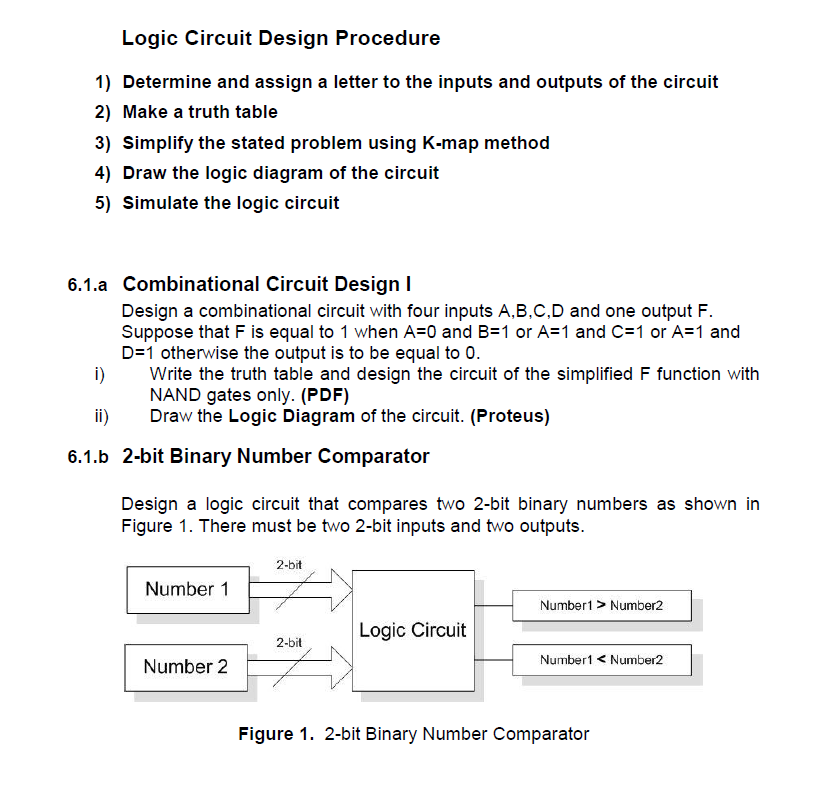
b bit Binary Number Comparator
Design a logic circuit that compares two bit binary numbers as shown in Figure There must be two bit inputs and two outputs.
Step by Step Solution
There are 3 Steps involved in it
1 Expert Approved Answer
Step: 1 Unlock

Question Has Been Solved by an Expert!
Get step-by-step solutions from verified subject matter experts
Step: 2 Unlock
Step: 3 Unlock