

Question: IC chips needed: 74155 (decoder), 7410 (3-input NAND), 74195 (4-bit shift register) Build the following and have the instructor check it. 1. A combinational

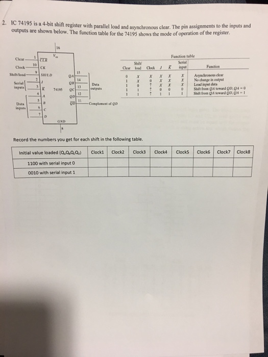
IC chips needed: 74155 (decoder), 7410 (3-input NAND), 74195 (4-bit shift register) Build the following and have the instructor check it. 1. A combinational circuit has 3 inputs: A, B and C, and one output F1. The simplified Boolean function for the circuit is FI(C, B, A) BA' + ABC Implement and test the combinational circuit, using a 74155 decoder IC and some external logic gates. The block diagram of the decoder and its truth table are shown below. When a 3x8 decoder is desired, inputs Cl and C2, as well as G1 and G2, must be connected together, as shown in the block diagram. G is the enable input and must be equal to 0 for proper operation. The 8 outputs are labeled with symbols given in the data book. The 74155 is using active low which means the selected output goes to 0 while all other outputs remain at 1. 100000oon C d. Derive the truth-table for F1 c. Draw the logic diagram for implementing F1 using a 3x8 decoder and a NAND gate f. Build the circuit using 74155, 7410 to verify your implementation 1000TTOOE A 0 1 0 1 0 1 0 1 F1 G 1 0 0 0 0 0 0 0 0 C x 0 Inputs B C 8 0 0 A 1 1 1 1 0 1 1 0 0 15 3 13 2 14 CI C2 B A GI G2 Vec 74155 GND Truth table A X X 0 0 0 1 0 1 0 1 1 0 1. 1 Fig 11-7 IC Type 74155 Connected as a 3 x 8 Decoder 1 1 210 293 212 213 IYO 111 192 193 1 E 1 1 1 1 I 1 1 0 1 Outputs 210 211 212 213 110 111 112 113 1 1 1 1 1 0 1 1 1 1 1 1 1 1 1 1 1 1 9 10 1 0 11 12 7 6 5 4 1 1 I 1 1 1 0 1 1 1 0 1 1 0 1 1 1 1 1 1 11 11 11 11 0 1 1 1 0 2. IC 74195 is a 4-bit shift register with parallel load and asynchronous clear. The pin assignments to the inputs and outputs are shown below. The function table for the 74195 shows the mode of operation of the register. Clear Clock Shift/load- Serial Data inputs 1 10 9 2 3 4 CLR CK 5 SH/LD J 6 7 8 16 D Va K 74195 A 15 QA 14 13 QC 12 QD 11 QD GND Data Initial value loaded (Q.QQQ) 1100 with serial input 0 0010 with serial input 1 outputs Complement of QD Shift Clear load 0 1 1 1 1 X X 0 I 1 Record the numbers you get for each shift in the following table. Clock1 Clock2 Clock3 Clock J X 0 t f T R X X X X X X 0 0 1 1 Function table Serial input Clock4 X X X 0 I Clocks Function Asynchronous clear No change in output Load input data Shift from QA toward QD, QA-0 Shift from QA toward QD, Q4-1 Clock6 Clock7 Clock8
Step by Step Solution
3.56 Rating (149 Votes )
There are 3 Steps involved in it
1 C 1 OO O 1 r O O 1 O B ... View full answer

Get step-by-step solutions from verified subject matter experts