

Question: Objectives: 1. To be able to design logic circuit using Universal NAND and NOR gate. Questions: Given the timing diagram given below, answer the following
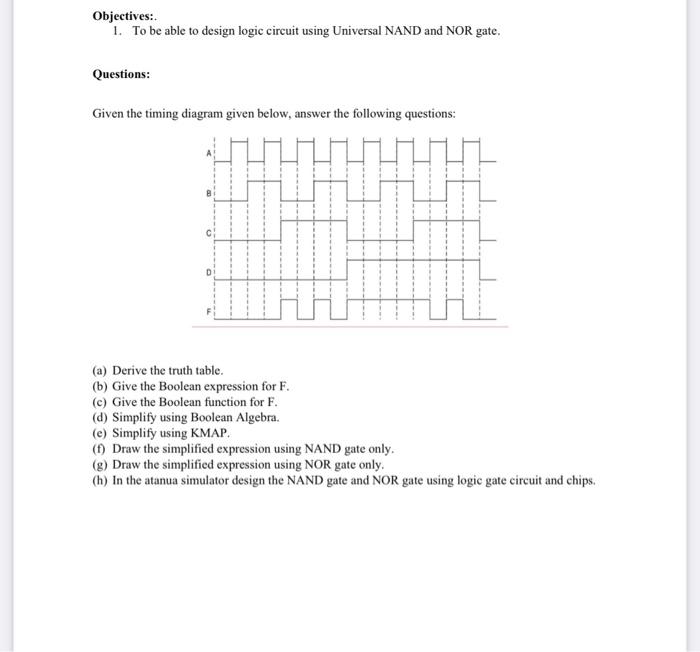
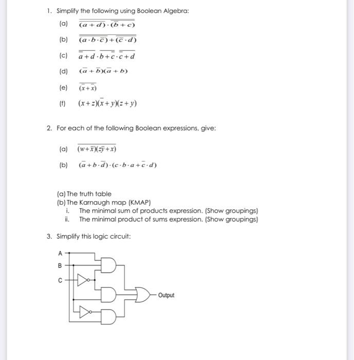
Objectives: 1. To be able to design logic circuit using Universal NAND and NOR gate. Questions: Given the timing diagram given below, answer the following questions: 1 D 1 (a) Derive the truth table. (b) Give the Boolean expression for F. (e) Give the Boolean function for F. (d) Simplify using Boolean Algebra (e) Simplify using KMAP. (f) Draw the simplified expression using NAND gate only. (g) Draw the simplified expression using NOR gate only. (h) In the atanua simulator design the NAND gate and NOR gate using logic gate circuit and chips. 1. Simplify the following using Boolean Algebra: (a) (a+d).(++) (b) (a b.)+(C.d) (c) a + d.b+c.c+d (a+ba+b) (d) (e) (x + x) (x + 2)(x + y): + y) () 2. For each of the following Boolean expressions, give: (a) (w+ x)27 + x) (b) (a+b-d)(c-b-a+c-d) (a) The truth table (b) The Karnaugh map (KMAP) i The minimal sum of products expression. (Show groupings) ii. The minimal product of sums expression. (Show groupings) 3. Simplify this logic circuit: A B Output
Step by Step Solution
There are 3 Steps involved in it

Get step-by-step solutions from verified subject matter experts