

Question: Please Please make the table for me I do not get it!!!!!!! Part I - Datapath Module: Data Path Table: Use this table determine which
Please Please make the table for me I do not get it!!!!!!!
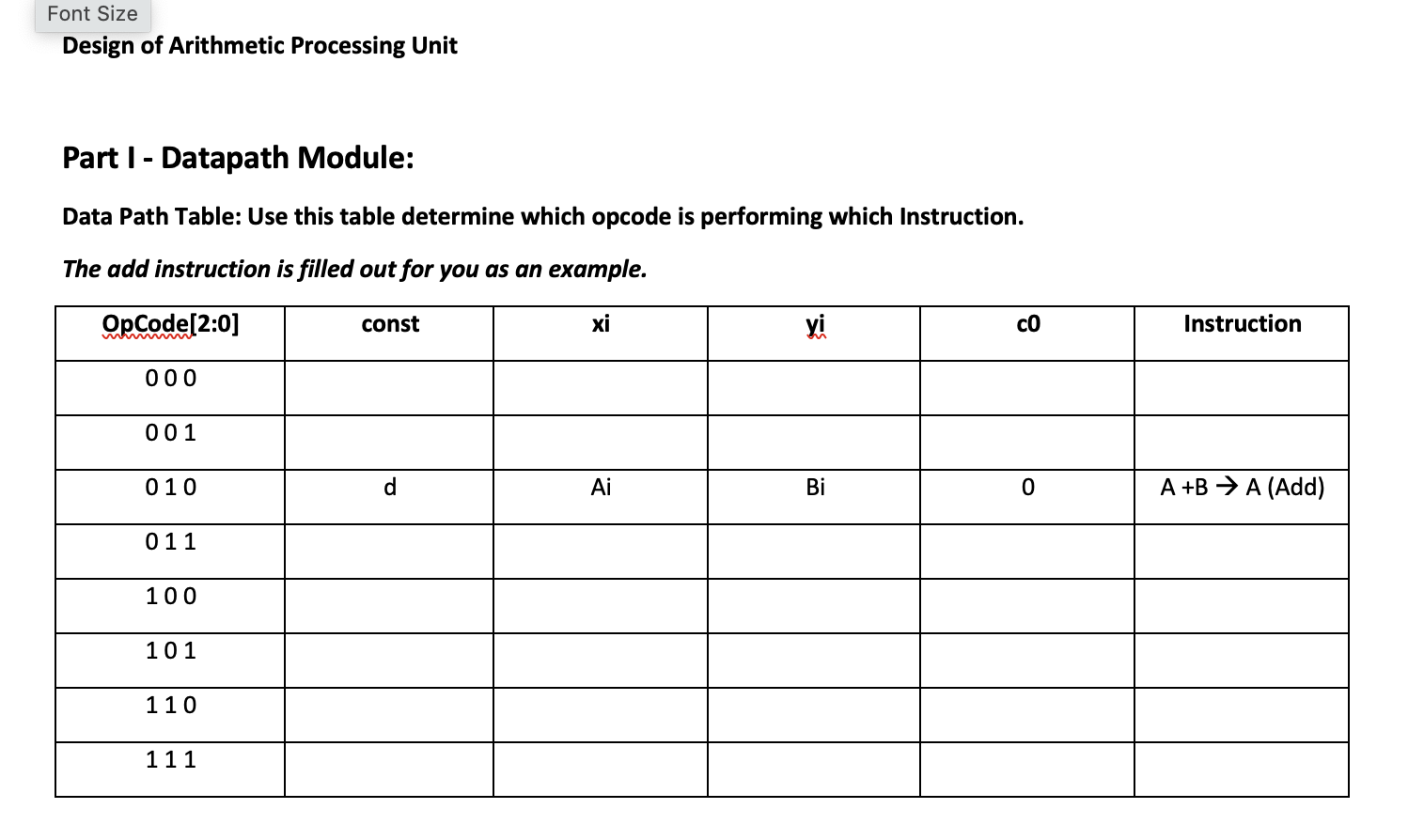
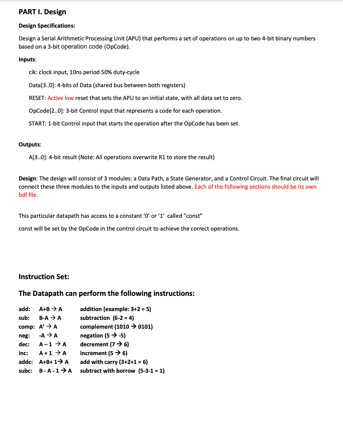
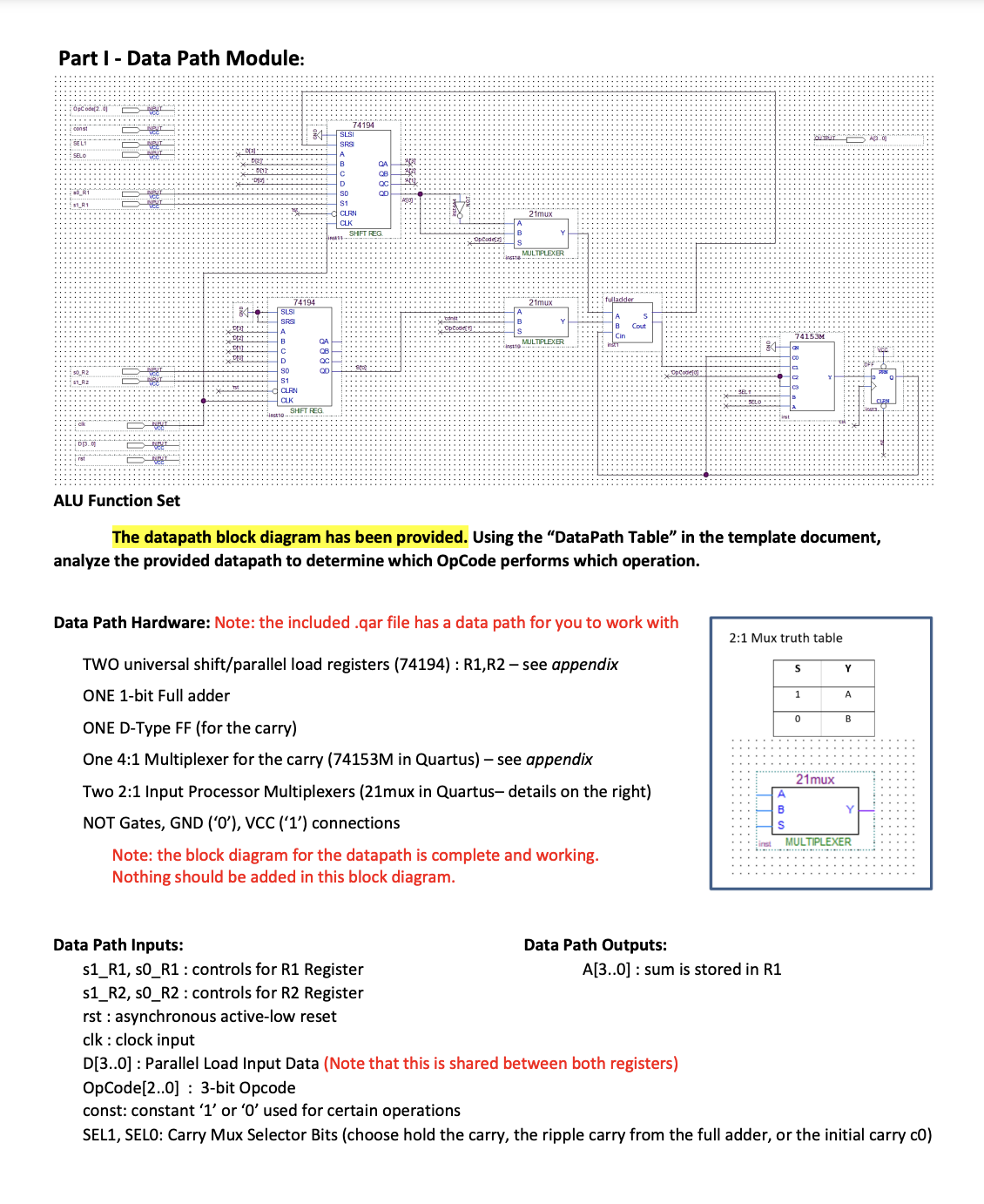
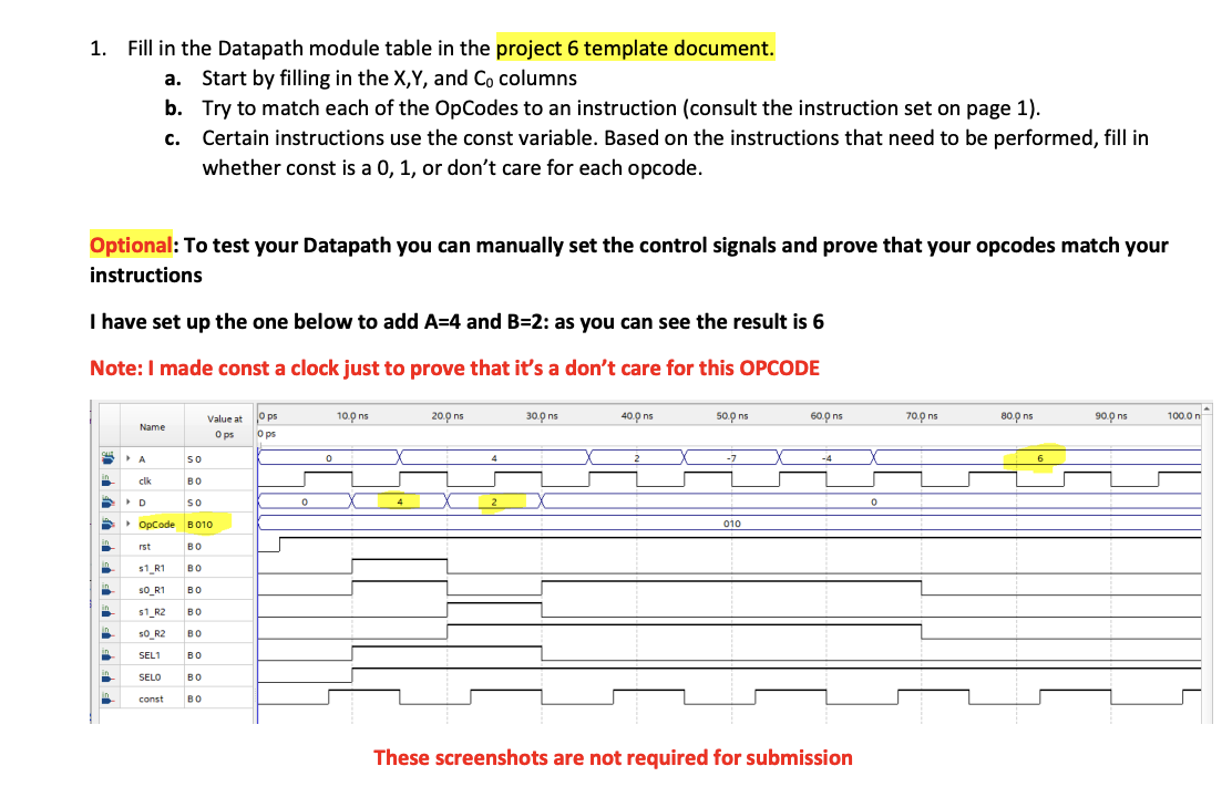
Part I - Datapath Module: Data Path Table: Use this table determine which opcode is performing which Instruction. The add instruction is filled out for you as an example. Design a Serial Arithmetic Processing Unit (APU) that performs a set of operations on up to two 4-bit binary numbers based on a 3-bit operation code (OpCode). Inputs: clk: clock input, 10 ns period 50% duty-cycle Data[3..0]: 4-bits of Data (shared bus between both registers) RESET: Active low reset that sets the APU to an initial state, with all data set to zero. OpCode[2..0]: 3-bit Control input that represents a code for each operation. START: 1-bit Control input that starts the operation after the OpCode has been set. Outputs: A[3..0]: 4-bit result (Note: All operations overwrite R1 to store the result) Design: The design will consist of 3 modules: a Data Path, a State Generator, and a Control Circuit. The final circuit will connect these three modules to the inputs and outputs listed above. Each of the following sections should be its own bdf file. This particular datapath has access to a constant ' 0 ' or ' 1 ' called "const" const will be set by the OpCode in the control circuit to achieve the correct operations. Instruction Set: The Datapath can perform the following instructions: add: A+BA addition (example: 3+2=5 ) sub: BAA subtraction (62=4) comp: AA complement (10100101) neg: AA negation (55) dec: A1A decrement (76) inc: A+1A increment (56) addc: A+B+1A add with carry (3+2+1=6) subc: BA1A subtract with borrow (531=1) Part I - Data Path Module: ALU Function Set The datapath block diagram has been provided. Using the "DataPath Table" in the template document, analyze the provided datapath to determine which OpCode performs which operation. Data Path Hardware: Note: the included .qar file has a data path for you to work with TWO universal shift/parallel load registers (74194) : R1,R2 - see appendix ONE 1-bit Full adder ONE D-Type FF (for the carry) One 4:1 Multiplexer for the carry (74153M in Quartus) - see appendix Two 2:1 Input Processor Multiplexers (21mux in Quartus- details on the right) NOT Gates, GND ('0'), VCC ('1') connections Note: the block diagram for the datapath is complete and working. Nothing should be added in this block diagram. Data Path Inputs: Data Path Outputs: s1_R1, s0_R1 : controls for R1 Register A[3..0] : sum is stored in R1 s1_R2, s0_R2 : controls for R2 Register rst : asynchronous active-low reset clk: clock input D[3..0] : Parallel Load Input Data (Note that this is shared between both registers) OpCode[2..0] : 3-bit Opcode const: constant ' 1 ' or ' 0 ' used for certain operations SEL1, SEL0: Carry Mux Selector Bits (choose hold the carry, the ripple carry from the full adder, or the initial carry c0) 1. Fill in the Datapath module table in the project 6 template document. a. Start by filling in the X,Y, and C0 columns b. Try to match each of the OpCodes to an instruction (consult the instruction set on page 1). c. Certain instructions use the const variable. Based on the instructions that need to be performed, fill in whether const is a 0,1 , or don't care for each opcode. Optional: To test your Datapath you can manually set the control signals and prove that your opcodes match your instructions I have set up the one below to add A=4 and B=2: as you can see the result is 6 Note: I made const a clock just to prove that it's a don't care for this OPCODE These screenshots are not required for submission
Step by Step Solution
There are 3 Steps involved in it

Get step-by-step solutions from verified subject matter experts