

Question: Please solve the following problem Q2. The micropatterns (first figure) can be achieved by KOH etching through the depth (550 um) of a (100) Si
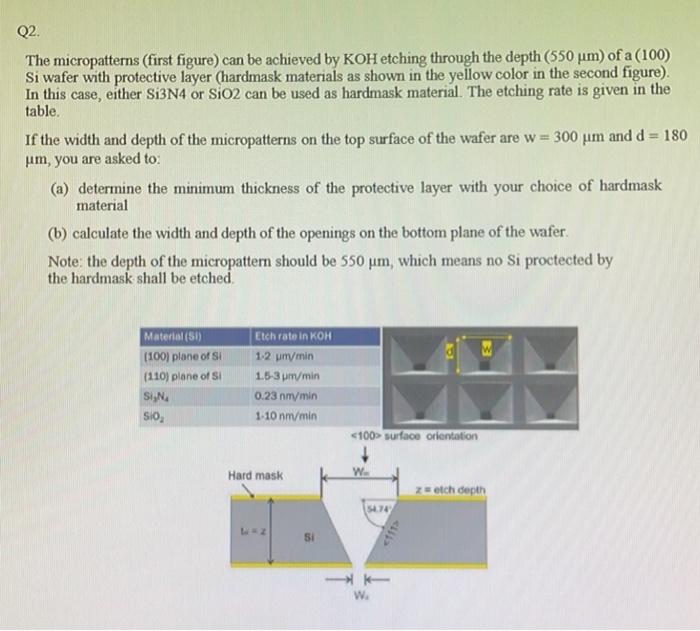
Q2. The micropatterns (first figure) can be achieved by KOH etching through the depth (550 um) of a (100) Si Wafer with protective layer (hardmask materials as shown in the yellow color in the second figure). In this case, either Si3N4 or SiO2 can be used as hardmask material. The etching rate is given in the table. If the width and depth of the micropatterns on the top surface of the wafer are w = 300 um and d = 180 uim, you are asked to (a) determine the minimum thickness of the protective layer with your choice of hardmask material (b) calculate the width and depth of the openings on the bottom plane of the wafer. Note: the depth of the micropattern should be 550 um, which means no Si proctected by the hardmask shall be etched Material (51) (100) plane of si (110) plane of Si SIN SIO Etch rate in KOH 1.2 um/min 1.5-3 m/min 0.23 nm/min 1-10 nm/min -100 surface orientation Hard mask W zetch depth 54.74 2 w
Step by Step Solution
There are 3 Steps involved in it

Get step-by-step solutions from verified subject matter experts