

Question: please write the following code in quartus prime please answer the questions too 3) Use the Quartus Prime Text Editor to implement a Behaviorally model
please write the following code in quartus prime

please answer the questions too
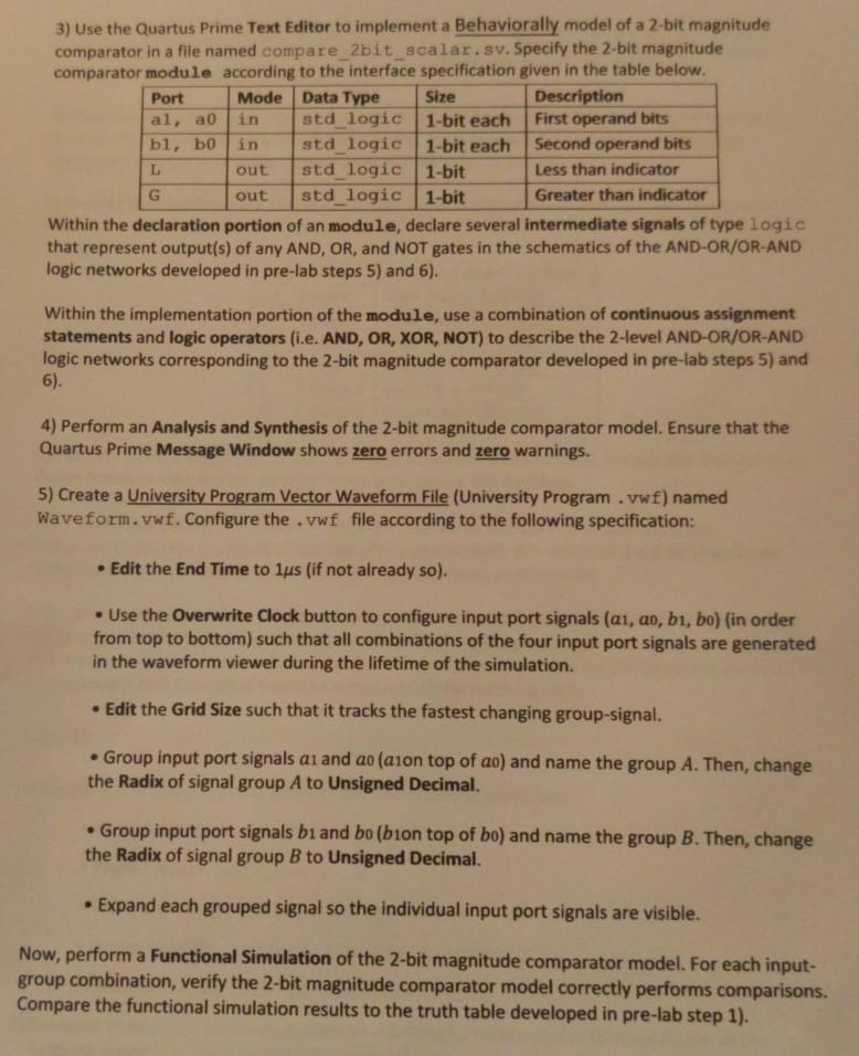
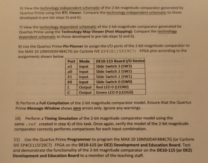
3) Use the Quartus Prime Text Editor to implement a Behaviorally model of a 2-bit magnitude comparator in a file named compare_2bit_scalar.sv. Specify the 2-bit magnitude comparator module according to the interface specification given in the table below. Port Mode Data Type Size Description al, ao in std_logic 1-bit each First operand bits bl, bo in std logic 1-bit each Second operand bits L out std logic 1-bit Less than indicator G out std logic 1-bit Greater than indicator Within the declaration portion of an module, declare several intermediate signals of type logic that represent output(s) of any AND, OR, and NOT gates in the schematics of the AND-OR/OR-AND logic networks developed in pre-lab steps 5) and 6). Within the implementation portion of the module, use a combination of continuous assignment statements and logic operators (i.e. AND, OR, XOR, NOT) to describe the 2-level AND-OR/OR-AND logic networks corresponding to the 2-bit magnitude comparator developed in pre-lab steps 5) and 6). 4) Perform an Analysis and Synthesis of the 2-bit magnitude comparator model. Ensure that the Quartus Prime Message Window shows zero errors and zero warnings. 5) Create a University Program Vector Waveform File (University Program .vwf) named Waveform.vwf. Configure the .vwf file according to the following specification: Edit the End Time to lus (if not already so). Use the Overwrite Clock button to configure input port signals (ai, ao, bi, bo) (in order from top to bottom) such that all combinations of the four input port signals are generated in the waveform viewer during the lifetime of the simulation. Edit the Grid Size such that it tracks the fastest changing group-signal. Group input port signals ai and ao (ason top of ac) and name the group A. Then, change the Radix of signal group A to Unsigned Decimal. Group input port signals bi and bo (bion top of bo) and name the group B. Then, change the Radix of signal group B to Unsigned Decimal. Expand each grouped signal so the individual input port signals are visible. Now, perform a Functional Simulation of the 2-bit magnitude comparator model. For each input- group combination, verify the 2-bit magnitude comparator model correctly performs comparisons. Compare the functional simulation results to the truth table developed in pre-lab step 1). 6) View the technology independent schematic of the 2-bit magnitude comparator generated by Quartus Prime using the RTL Viewer. Compare the technology independent schematic to those developed in pre-lab steps 5) and 6). 7) View the technology dependent schematic of the 2-bit magnitude comparator generated by Quartus Prime using the Technology Map Viewer (Post Mapping). Compare the technology dependent schematic to those developed in pre-lab steps 5) and 6). 8) Use the Quartus Prime Pin Planner to assign the I/O ports of the 2-bit magnitude comparator to the MAX 10 10MSODAF484C7G (or Cyclone IVE EP4CE115F2907) FPGA pins according to the assignments shown below. Port Mode DE10-115 Board I/O Device al Input Slide Switch 3 (SW3) a0 Input Slide Switch 2 (SW2) b1 Input Slide Switch 1 (SW1) bo Input Slide Switch O (SWO) L Output Red LED O (LEDRO) G Output Green LED O (LEDGO) 9) Perform a Full Compilation of the 2-bit magnitude comparator model. Ensure that the Quartus Prime Message Window shows zero errors only. Ignore any warnings. 10) Perform a Timing Simulation of the 2-bit magnitude comparator model using the same.vwf created in step 4) of this task. Once again, verify the model of the 2-bit magnitude comparator correctly performs comparisons for each input combination. 11) Use the Quartus Prime Programmer to program the MAX 10 10M5ODAF484C7G (or Cyclone IVE EP4CE115F2907) FPGA on the DE10-115 (or DE2) Development and Education Board. Test and demonstrate the functionality of the 2-bit magnitude comparator on the DE10-115 (or DE2) Development and Education Board to a member of the teaching staff. 1) How many logic elements (Les) (as a number and as a percentage) are used to realize the 2-bit magnitude comparator on the MAX 10 10M50 DAF 48407G (or Cyclone IVE EP4CE115F2907) FPGA? 2) What is the smallest and largest observable delay in the output port signals L and G for the 2-bit magnitude comparator? 3) Compare the RTL Viewer technology independent schematic viewed in procedure step 5) with the schematic developed in pre-lab steps 5) and 6). What is similar? What is different? Why? 3) Use the Quartus Prime Text Editor to implement a Behaviorally model of a 2-bit magnitude comparator in a file named compare_2bit_scalar.sv. Specify the 2-bit magnitude comparator module according to the interface specification given in the table below. Port Mode Data Type Size Description al, ao in std_logic 1-bit each First operand bits bl, bo in std logic 1-bit each Second operand bits L out std logic 1-bit Less than indicator G out std logic 1-bit Greater than indicator Within the declaration portion of an module, declare several intermediate signals of type logic that represent output(s) of any AND, OR, and NOT gates in the schematics of the AND-OR/OR-AND logic networks developed in pre-lab steps 5) and 6). Within the implementation portion of the module, use a combination of continuous assignment statements and logic operators (i.e. AND, OR, XOR, NOT) to describe the 2-level AND-OR/OR-AND logic networks corresponding to the 2-bit magnitude comparator developed in pre-lab steps 5) and 6). 4) Perform an Analysis and Synthesis of the 2-bit magnitude comparator model. Ensure that the Quartus Prime Message Window shows zero errors and zero warnings. 5) Create a University Program Vector Waveform File (University Program .vwf) named Waveform.vwf. Configure the .vwf file according to the following specification: Edit the End Time to lus (if not already so). Use the Overwrite Clock button to configure input port signals (ai, ao, bi, bo) (in order from top to bottom) such that all combinations of the four input port signals are generated in the waveform viewer during the lifetime of the simulation. Edit the Grid Size such that it tracks the fastest changing group-signal. Group input port signals ai and ao (ason top of ac) and name the group A. Then, change the Radix of signal group A to Unsigned Decimal. Group input port signals bi and bo (bion top of bo) and name the group B. Then, change the Radix of signal group B to Unsigned Decimal. Expand each grouped signal so the individual input port signals are visible. Now, perform a Functional Simulation of the 2-bit magnitude comparator model. For each input- group combination, verify the 2-bit magnitude comparator model correctly performs comparisons. Compare the functional simulation results to the truth table developed in pre-lab step 1). 6) View the technology independent schematic of the 2-bit magnitude comparator generated by Quartus Prime using the RTL Viewer. Compare the technology independent schematic to those developed in pre-lab steps 5) and 6). 7) View the technology dependent schematic of the 2-bit magnitude comparator generated by Quartus Prime using the Technology Map Viewer (Post Mapping). Compare the technology dependent schematic to those developed in pre-lab steps 5) and 6). 8) Use the Quartus Prime Pin Planner to assign the I/O ports of the 2-bit magnitude comparator to the MAX 10 10MSODAF484C7G (or Cyclone IVE EP4CE115F2907) FPGA pins according to the assignments shown below. Port Mode DE10-115 Board I/O Device al Input Slide Switch 3 (SW3) a0 Input Slide Switch 2 (SW2) b1 Input Slide Switch 1 (SW1) bo Input Slide Switch O (SWO) L Output Red LED O (LEDRO) G Output Green LED O (LEDGO) 9) Perform a Full Compilation of the 2-bit magnitude comparator model. Ensure that the Quartus Prime Message Window shows zero errors only. Ignore any warnings. 10) Perform a Timing Simulation of the 2-bit magnitude comparator model using the same.vwf created in step 4) of this task. Once again, verify the model of the 2-bit magnitude comparator correctly performs comparisons for each input combination. 11) Use the Quartus Prime Programmer to program the MAX 10 10M5ODAF484C7G (or Cyclone IVE EP4CE115F2907) FPGA on the DE10-115 (or DE2) Development and Education Board. Test and demonstrate the functionality of the 2-bit magnitude comparator on the DE10-115 (or DE2) Development and Education Board to a member of the teaching staff. 1) How many logic elements (Les) (as a number and as a percentage) are used to realize the 2-bit magnitude comparator on the MAX 10 10M50 DAF 48407G (or Cyclone IVE EP4CE115F2907) FPGA? 2) What is the smallest and largest observable delay in the output port signals L and G for the 2-bit magnitude comparator? 3) Compare the RTL Viewer technology independent schematic viewed in procedure step 5) with the schematic developed in pre-lab steps 5) and 6). What is similar? What is different? Why
Step by Step Solution
There are 3 Steps involved in it

Get step-by-step solutions from verified subject matter experts