

Question: Q1/ Design a circuit that has two inputs X, and S, where X represents an 8-bit BCD number, S is a sign bit. The circuit
Q1/ Design a circuit that has two inputs X, and S, where X represents an 8-bit BCD number, S is a sign bit. The circuit has one output Y, which is the Binary representation of the signed-magnitude BCD number. A negative output is represented in the Binary 2scomplement form. You need to think of two design alternatives.
(design 2) :
.
, .
, ( ) .
- .
Requirements:
- Draw the (design 2) block diagram and explain how you did it in order
#example of (block diagram) for different design
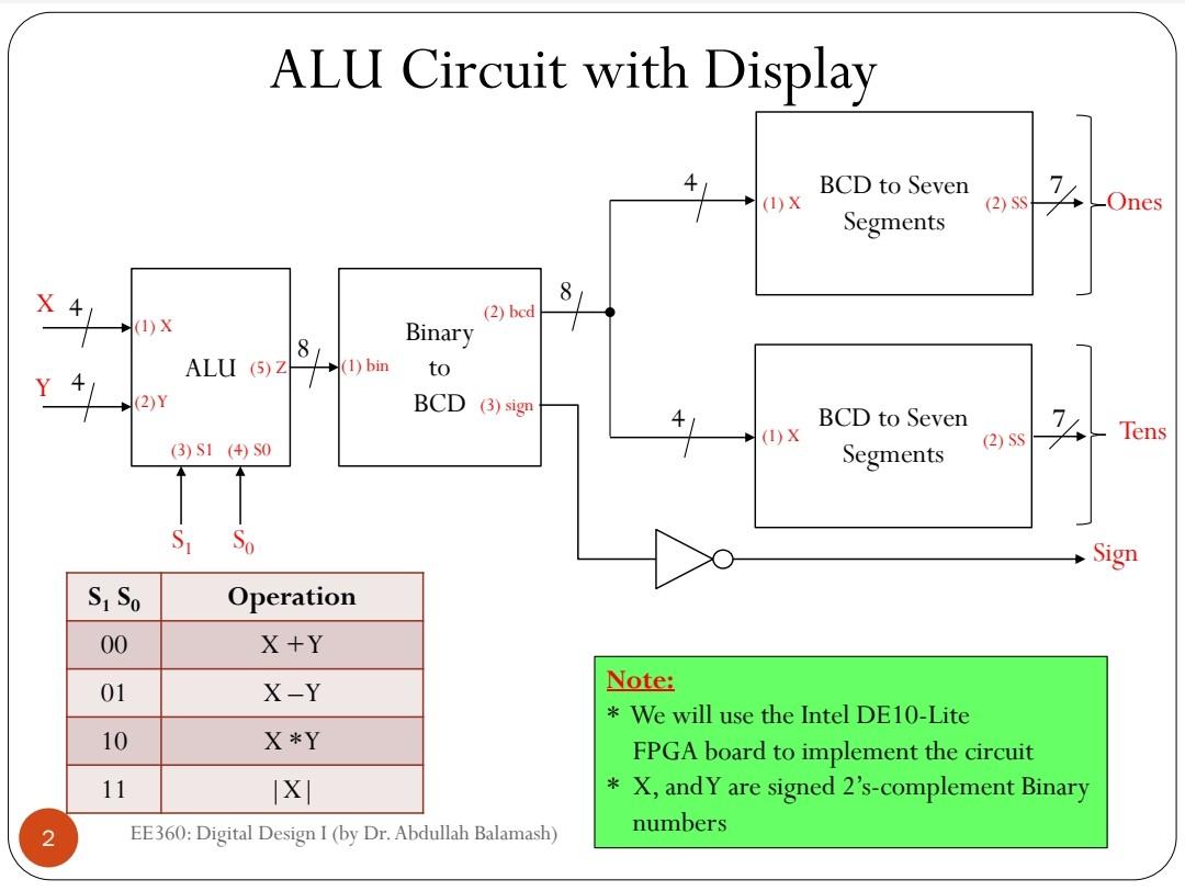
ALU Circuit with Display \begin{tabular}{|c|c|} \hline S1S0 & Operation \\ \hline 00 & X+Y \\ \hline 01 & XY \\ \hline 10 & XY \\ \hline 11 & X \\ \hline \end{tabular} Note: * We will use the Intel DE10-Lite FPGA board to implement the circuit * X, and Y are signed 2's-complement Binary 2 numbers
Step by Step Solution
There are 3 Steps involved in it

Get step-by-step solutions from verified subject matter experts