

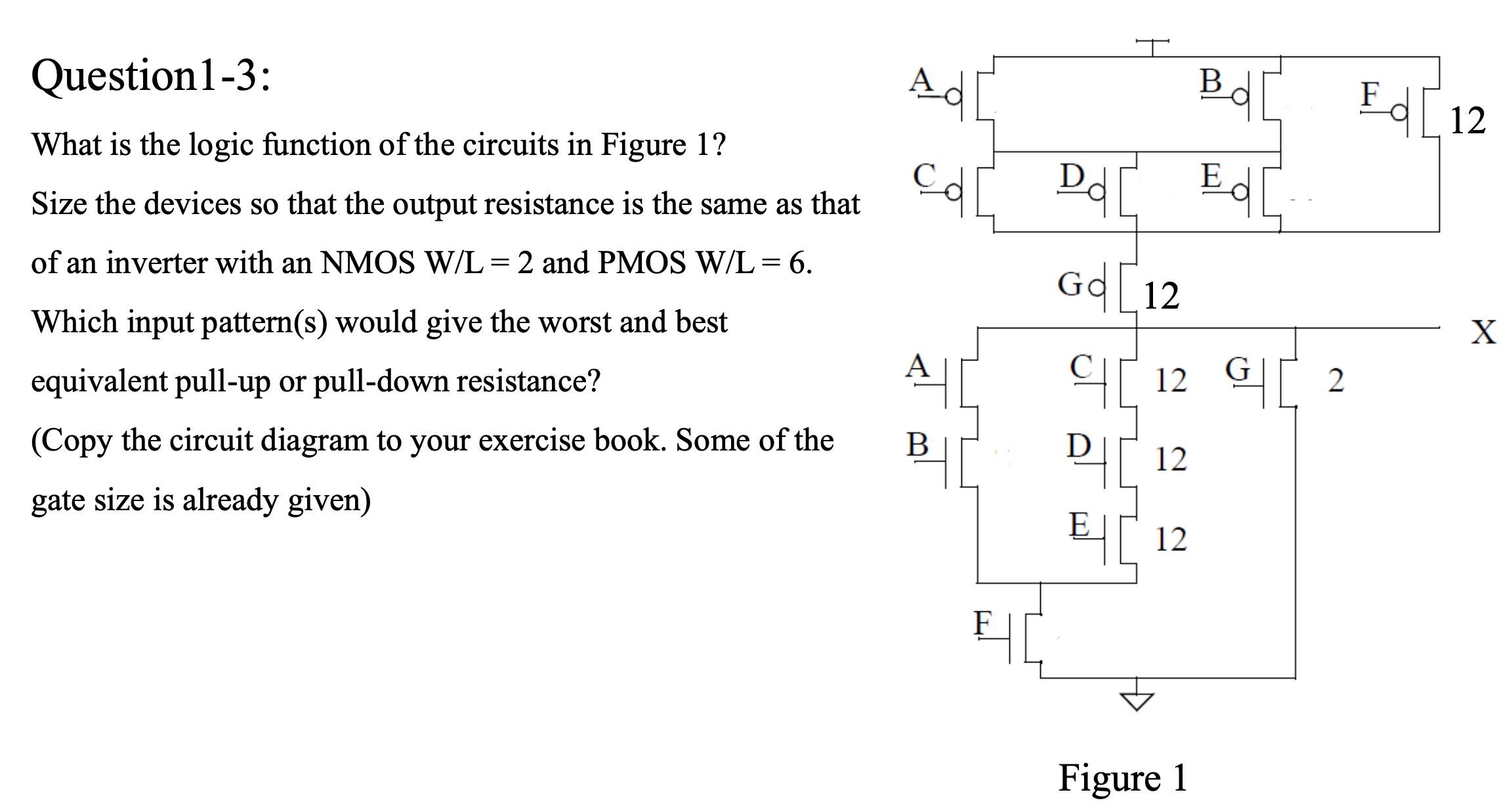
Question: Question 1 - 3 : What is the logic function of the circuits in Figure 1 ? Size the devices so that the output resistance
Question:
What is the logic function of the circuits in Figure
Size the devices so that the output resistance is the same as that of an inverter with an NMOS mathrmWmathrmL and mathrmPMOSmathrmWmathrmL
Which input patterns would give the worst and best equivalent pullup or pulldown resistance?
Copy the circuit diagram to your exercise book. Some of the gate size is already given
Figure
Step by Step Solution
There are 3 Steps involved in it
1 Expert Approved Answer
Step: 1 Unlock

Question Has Been Solved by an Expert!
Get step-by-step solutions from verified subject matter experts
Step: 2 Unlock
Step: 3 Unlock