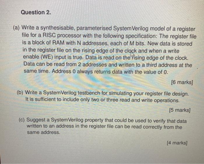
Question: Question 2. (a) Write a synthesisable, parameterised System Verilog model of a register file for a RISC processor with the following specification: The register file

Question 2. (a) Write a synthesisable, parameterised System Verilog model of a register file for a RISC processor with the following specification: The register file is a block of RAM with N addresses, each of M bits. New data is stored in the register file on the rising edge of the clock and when a write enable (WE) input is true. Data is read on the Fising edge of the clock. Data can be read from 2 addresses and written to a third address at the same time. Address 0 always returns data with the value of 0. [6 marks] (b) Write a System Verilog testbench for simulating your register file design. It is sufficient to include only two or three read and write operations. [5 marks] (c) Suggest a System Verilog property that could be used to verify that data written to an address in the register file can be read correctly from the same address. [4 marks] Question 2. (a) Write a synthesisable, parameterised System Verilog model of a register file for a RISC processor with the following specification: The register file is a block of RAM with N addresses, each of M bits. New data is stored in the register file on the rising edge of the clock and when a write enable (WE) input is true. Data is read on the Fising edge of the clock. Data can be read from 2 addresses and written to a third address at the same time. Address 0 always returns data with the value of 0. [6 marks] (b) Write a System Verilog testbench for simulating your register file design. It is sufficient to include only two or three read and write operations. [5 marks] (c) Suggest a System Verilog property that could be used to verify that data written to an address in the register file can be read correctly from the same address. [4 marks]
Step by Step Solution
There are 3 Steps involved in it

Get step-by-step solutions from verified subject matter experts


