

Question: Question 4 (24 Points)-Register Design a 3-bit shift register with 2 control inputs C1 and CO, using three cos flip-flops and three 4x1 multiplexers. Data
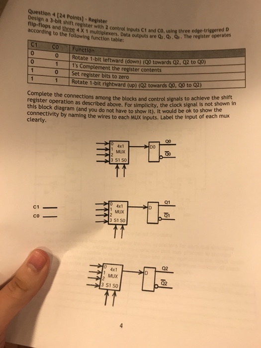
Question 4 (24 Points)-Register Design a 3-bit shift register with 2 control inputs C1 and CO, using three cos flip-flops and three 4x1 multiplexers. Data outputs are Qi. Qs.QThe according to the following function table: edge-triggered D register operates C1 C0 Function 0 |Rotate 1-bit leftward (downl (Qo towards Q2,Q2 to co 1 1's Complement the register contents 0 Set register bits to zero Rotate 1-bit rightward (up)(Q2towardsQ ,QOtoQ2) ete the connections among the blocks and control signals to achieve the shift register operation as described above. For simplicity, the clock signal is not shown in his block diagram (and you do not have to show it). It would be ok to show the connectivity by naming the wires to each MUX inputs. Labet the clearly input of each mux 0 4x1 1 MUX Do 3 S1 SO Q1 0 4x1 Q2 3 S1 SO Question 4 (24 Points)-Register Design a 3-bit shift register with 2 control inputs C1 and CO, using three cos flip-flops and three 4x1 multiplexers. Data outputs are Qi. Qs.QThe according to the following function table: edge-triggered D register operates C1 C0 Function 0 |Rotate 1-bit leftward (downl (Qo towards Q2,Q2 to co 1 1's Complement the register contents 0 Set register bits to zero Rotate 1-bit rightward (up)(Q2towardsQ ,QOtoQ2) ete the connections among the blocks and control signals to achieve the shift register operation as described above. For simplicity, the clock signal is not shown in his block diagram (and you do not have to show it). It would be ok to show the connectivity by naming the wires to each MUX inputs. Labet the clearly input of each mux 0 4x1 1 MUX Do 3 S1 SO Q1 0 4x1 Q2 3 S1 SO
Step by Step Solution
There are 3 Steps involved in it

Get step-by-step solutions from verified subject matter experts