

Question: Question 4. We obtained a power diffraction pattern from an unknown sample and the data is attached. The sample has a cubic symmetry. (a) Determine
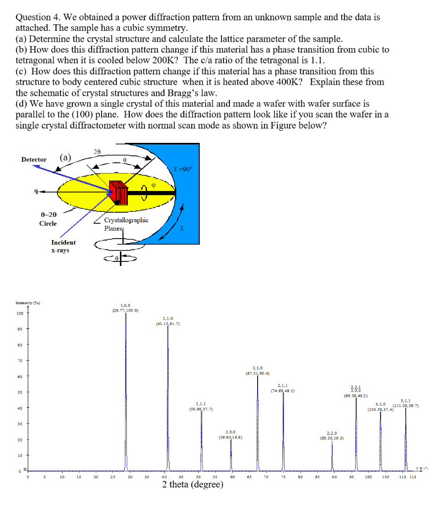
Question 4. We obtained a power diffraction pattern from an unknown sample and the data is attached. The sample has a cubic symmetry. (a) Determine the crystal structure and calculate the lattice parameter of the sample. (b) How does this diffraction pattern change if this material has a phase transition from cubic to tetragonal when it is cooled below 200K? The c/a ratio of the tetragonal is 1.1. (c) How does this diffraction pattern change if this material has a phase transition from this structure to body centered cubic structure when it is heated above 400K? Explain these from the schematic of crystal structures and Bragg's law. (d) We have grown a single crystal of this material and made a wafer with wafer surface is parallel to the (100) plane. How does the diffraction pattern look like if you scan the wafer in a single crystal diffractometer with normal scan mode as shown in Figure below? 20 Detector (a) X =90 0-20 Circle Crystallographic Planes Incident X-rays Intensity) 1.0.0 Q28.77.100.0) 100 1.1.0 (41.15,91.7) 90 80 70 2.1.0 (67.51,60.4) 60 2.1.1 (74.98,40.1) 50 3.2:6 (96.39, 46.2) 3.1.1 3.1.0 (211.00.30.7) (103.58,37.4) 40 1.1.1 (50.98.37.7) 30 2.0.0 () (59.60,19.8) 2.2.0 (89.30, 19.3) 20 10 - O" 0 D 3 10 15 20 25 30 33 40 45 5035 00 os 70 75 80 85 90 95 100 105 110 113 2 theta (degree) Question 4. We obtained a power diffraction pattern from an unknown sample and the data is attached. The sample has a cubic symmetry. (a) Determine the crystal structure and calculate the lattice parameter of the sample. (b) How does this diffraction pattern change if this material has a phase transition from cubic to tetragonal when it is cooled below 200K? The c/a ratio of the tetragonal is 1.1. (c) How does this diffraction pattern change if this material has a phase transition from this structure to body centered cubic structure when it is heated above 400K? Explain these from the schematic of crystal structures and Bragg's law. (d) We have grown a single crystal of this material and made a wafer with wafer surface is parallel to the (100) plane. How does the diffraction pattern look like if you scan the wafer in a single crystal diffractometer with normal scan mode as shown in Figure below? 20 Detector (a) X =90 0-20 Circle Crystallographic Planes Incident X-rays Intensity) 1.0.0 Q28.77.100.0) 100 1.1.0 (41.15,91.7) 90 80 70 2.1.0 (67.51,60.4) 60 2.1.1 (74.98,40.1) 50 3.2:6 (96.39, 46.2) 3.1.1 3.1.0 (211.00.30.7) (103.58,37.4) 40 1.1.1 (50.98.37.7) 30 2.0.0 () (59.60,19.8) 2.2.0 (89.30, 19.3) 20 10 - O" 0 D 3 10 15 20 25 30 33 40 45 5035 00 os 70 75 80 85 90 95 100 105 110 113 2 theta (degree)
Step by Step Solution
There are 3 Steps involved in it

Get step-by-step solutions from verified subject matter experts