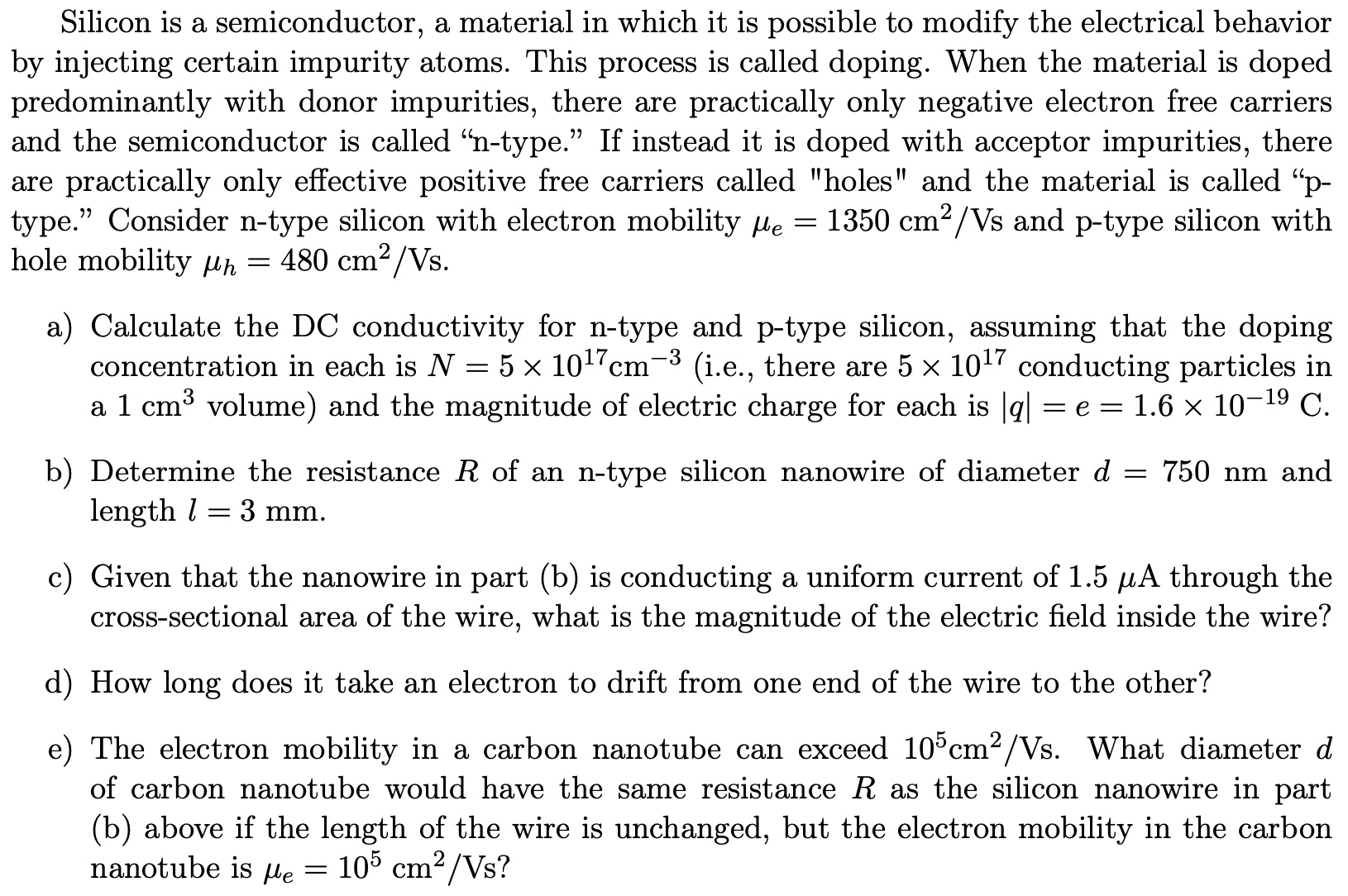
Question: Silicon is a semiconductor, a material in which it is possible to modify the electrical behavior by injecting certain impurity atoms. This process is called

Silicon is a semiconductor, a material in which it is possible to modify the electrical behavior by injecting certain impurity atoms. This process is called dOping. When the material is dOped predominantly with donor impurities, there are practically only negative electron free carriers and the semiconductor is called \"n-type.\" If instead it is doped with acceptor impurities, there are practically only effective positive free carriers called "holes" and the material is called \"p type.\" Consider ntype silicon with electron mobility pa = 1350 cm2/Vs and ptype silicon with hole mobility m, = 480 cm2/Vs. a) Calculate the DC conductivity for ntype and p-type silicon, assuming that the doping concentration in each is N = 5 X 1017cm_3 (i.e., there are 5 x 10¹⁷ conducting particles in a 1 cm3 volume) and the magnitude of electric charge for each is |q| = e = 1.6 X 10¹⁹ C. b) Determine the resistance R of an ntype silicon nanowire of diameter d = 750 nm and length l = 3 mm. c) Given that the nanowire in part (b) is conducting a uniform current of 1.5 MA through the cross-sectional area of the wire, what is the magnitude of the electric eld inside the wire? d) How long does it take an electron to drift from one end of the wire to the other? e) The electron mobility in a carbon nanotube can exceed 105cm2/Vs. What diameter d of carbon nanotube would have the same resistance R as the silicon nanowire in part (b) above if the length of the wire is unchanged, but the electron mobility in the carbon nanotube is [.56 : 105 cm2/Vs
Step by Step Solution
There are 3 Steps involved in it

Get step-by-step solutions from verified subject matter experts


