

T- en clock J C cir M EE598 Verilog Design Q Q' INPUT INBUT Q Q'...
Fantastic news! We've Found the answer you've been seeking!
Question:
![clock 89899 cir en Q1 02 Ops 25 ns clk enable reset inst 5.12 us count_out[2..0] Figure 4 C 10.24 us Figure 3](https://dsd5zvtm8ll6.cloudfront.net/si.experts.images/answers/2023/10/651dae0f7abf6_918651dae0eebc0c.jpg)
![InClass Exercise 2 cik enable reset clk three_bit_counter Ops 5 ns count_out[2] count_out[1] count_out[0] clk](https://dsd5zvtm8ll6.cloudfront.net/si.experts.images/answers/2023/10/651dae10a5079_920651dae10055da.jpg)
Transcribed Image Text:
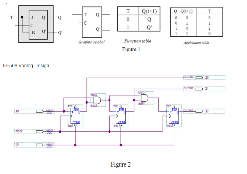
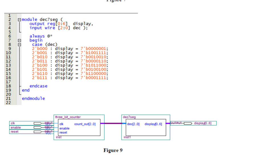
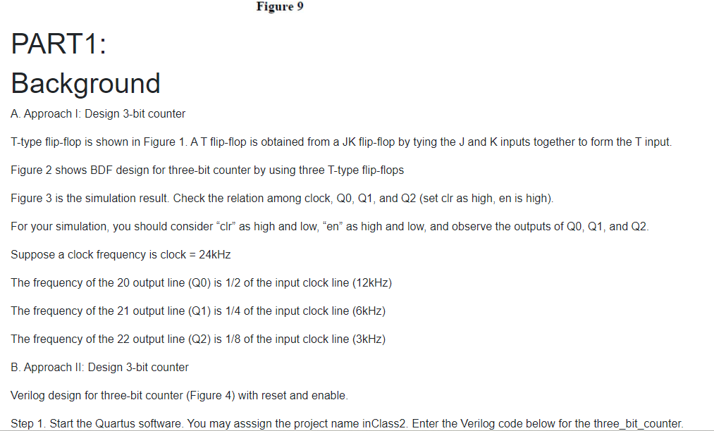
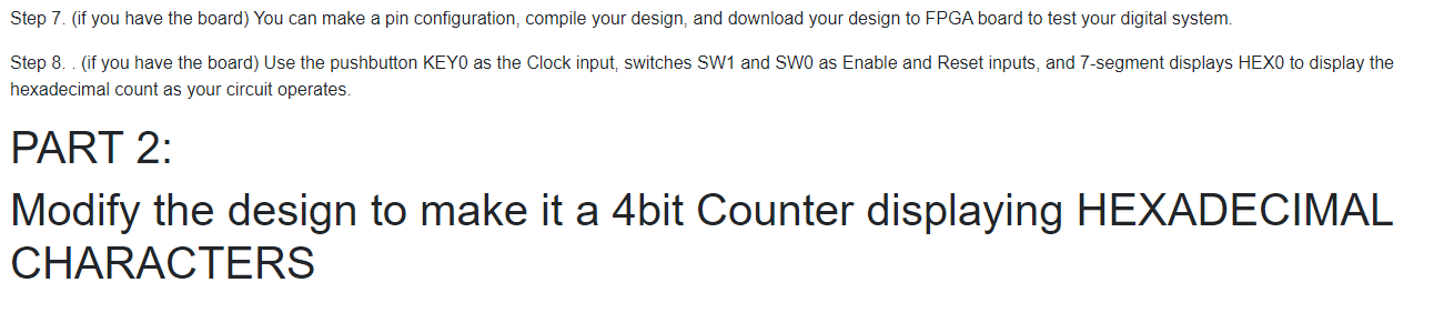
T- en clock J C cir M EE598 Verilog Design Q Q' "INPUT INBUT Q Q' TFF PRN T T Graphic symbol CLBN Q AND2 TFF T CLBN inst T 0 1 Function table Figure 1 Q(t+1) Q Q' Figure 2 JANDZ ins14 STEF Q Q(+1) 0 1 0 1 0 0 1 1 LEN PROMBOY Application table OUTPUT k T 0 1 OUTPUT 0 Q1 Q2 clock 89899 cir en Q1 02 Ops 25 ns clk enable reset inst 5.12 us count_out[2..0] Figure 4 C 10.24 us Figure 3 15.36 us 20.0 us InClass Exercise 2 cik enable reset clk three_bit_counter Ops 5 ns count_out[2] count_out[1] count_out[0] clk enable reset inst Figure 6 Designing a Multi-bit Counter and Programming on DE10-Lite count_out[2..0] 5.12 us 10.24 us reset enable count_out @[11X121 (13) (41) (51) (161) (71X10X12X OUTPUT ת 15.36 us count_out[2..01 Figure 7 20.48 us பாப 101 25. us 30.0 us LLLLAAAANNN 890000 VOSTWNTOCOLOSAWNT 2 3 9 10 11 12 13 14 15 16 17 18 19 20 00 22 module dec7seg ( cik enable reset output reg[0:6] display, input wire [2:0] dec );" always @* begin case (dec) end 2'b000 2 b001 2 b010 2 b011 2 b100 2'b101 2 b110 2'b111: 21 endmodule endcase INPUT MWEZ INPUT Wala INPUT WEE = display 7'b0000001; display = 7'b1001111; display = 7'b0010010; display = 7'b0000110; display = 7'b1011000; display = 7'b0100100; display = 7'b1100000; display = 7'b0001111; three_bit_counter clk enable reset inst count_out[2..0] Figure 9 dec7seg dec[2..0] display[0..6] insti OUTPUT display(0..6] Figure 9 PART 1: Background A. Approach I: Design 3-bit counter T-type flip-flop is shown in Figure 1. A T flip-flop is obtained from a JK flip-flop by tying the J and K inputs together to form the T input. Figure 2 shows BDF design for three-bit counter by using three T-type flip-flops Figure 3 is the simulation result. Check the relation among clock, QO, Q1, and Q2 (set clr as high, en is high). For your simulation, you should consider "clr" as high and low, "en" as high and low, and observe the outputs of Q0, Q1, and Q2. Suppose a clock frequency is clock = 24kHz The frequency of the 20 output line (Q0) is 1/2 of the input clock line (12kHz) The frequency of the 21 output line (Q1) is 1/4 of the input clock line (6kHz) The frequency of the 22 output line (Q2) is 1/8 of the input clock line (3kHz) B. Approach II: Design 3-bit counter Verilog design for three-bit counter (Figure 4) with reset and enable. Step 1. Start the Quartus software. You may asssign the project name inClass2. Enter the Verilog code below for the three_bit_counter. Step 3. Save the Verilog file (Figure 5) as three_bit_counter.v as part of our project under your subfolder. Place a check mark in the space labeled Add file to current project and press Save Step 4. Select File - Create/Update - Create Symbol Files for Current File (three_bit_counter.bsf symbol) to create a symbol file for the Verilog code entered. A Compilation Report window initially displays "Report not available"; however, be patient. A display window should soon appear stating that the Create Symbol File was (or not) successful. Click OK and close the Compilation Report window. Step 5. Open a new Schematic file (File > New) by highlighting Block Diagram/Schematic File. And click OK. Find the symbol file (bsf file you just created for Verilog in Step 4) from Project folder to support your design in BDF view. Insert the symbol and input/output pins. Note that multi-bit buses "Properties" must be used to rename the port signal as <name> [MSB..LSB]. In our case, count_out[2..0] will be the correct format. Step 6. Before compiling this bdf file, we need to name this bdf file and save it as part of our project under your subfolder. Choose File > Save As and enter File name as counter3. Place a check mark in the space labeled Add file to current project and press Save. Step 7. create a Vector Waveform File (vwf) to simulate a design(bdf) file. Set an end time 30 µs for simulation from Edit and then run simulation based on Figure 3. You may have to expand the size of the Simulation Waveforms to suit your need and choose View > Fit in Window to see the entire 30µs waveform. Figure 7 is the simulation result. Check the relation among clock, reset, enable, count_out[0], count_out[1], count_out[2]. Integrate the decoder with 3-bit counter Step 1. design a decoder in Verilog (Figure 8) Step 2. Save the Verilog file as dec7seg v as part of our project under your subfolder. Place a check mark in the space labeled Add file to current project and press Save Step 3. Select File - Create/Update - Create Symbol Files for Current File (dec7seg.bsf symbol) to create a symbol file for the Verilog code entered. Step 4. Open a new Schematic file (File > New) by highlighting Block Diagram/Schematic File. And click OK. Find the symbol file (bsf file you created for Verilog) from Project folder to support your design in BDF view. Insert the symbol and input/output pins Step 7. (if you have the board) You can make a pin configuration, compile your design, and download your design to FPGA board to test your digital system. Step 8.. (if you have the board) Use the pushbutton KEYO as the Clock input, switches SW1 and SWO as Enable and Reset inputs, and 7-segment displays HEXO to display the hexadecimal count as your circuit operates. PART 2: Modify the design to make it a 4bit Counter displaying HEXADECIMAL CHARACTERS T- en clock J C cir M EE598 Verilog Design Q Q' "INPUT INBUT Q Q' TFF PRN T T Graphic symbol CLBN Q AND2 TFF T CLBN inst T 0 1 Function table Figure 1 Q(t+1) Q Q' Figure 2 JANDZ ins14 STEF Q Q(+1) 0 1 0 1 0 0 1 1 LEN PROMBOY Application table OUTPUT k T 0 1 OUTPUT 0 Q1 Q2 clock 89899 cir en Q1 02 Ops 25 ns clk enable reset inst 5.12 us count_out[2..0] Figure 4 C 10.24 us Figure 3 15.36 us 20.0 us InClass Exercise 2 cik enable reset clk three_bit_counter Ops 5 ns count_out[2] count_out[1] count_out[0] clk enable reset inst Figure 6 Designing a Multi-bit Counter and Programming on DE10-Lite count_out[2..0] 5.12 us 10.24 us reset enable count_out @[11X121 (13) (41) (51) (161) (71X10X12X OUTPUT ת 15.36 us count_out[2..01 Figure 7 20.48 us பாப 101 25. us 30.0 us LLLLAAAANNN 890000 VOSTWNTOCOLOSAWNT 2 3 9 10 11 12 13 14 15 16 17 18 19 20 00 22 module dec7seg ( cik enable reset output reg[0:6] display, input wire [2:0] dec );" always @* begin case (dec) end 2'b000 2 b001 2 b010 2 b011 2 b100 2'b101 2 b110 2'b111: 21 endmodule endcase INPUT MWEZ INPUT Wala INPUT WEE = display 7'b0000001; display = 7'b1001111; display = 7'b0010010; display = 7'b0000110; display = 7'b1011000; display = 7'b0100100; display = 7'b1100000; display = 7'b0001111; three_bit_counter clk enable reset inst count_out[2..0] Figure 9 dec7seg dec[2..0] display[0..6] insti OUTPUT display(0..6] Figure 9 PART 1: Background A. Approach I: Design 3-bit counter T-type flip-flop is shown in Figure 1. A T flip-flop is obtained from a JK flip-flop by tying the J and K inputs together to form the T input. Figure 2 shows BDF design for three-bit counter by using three T-type flip-flops Figure 3 is the simulation result. Check the relation among clock, QO, Q1, and Q2 (set clr as high, en is high). For your simulation, you should consider "clr" as high and low, "en" as high and low, and observe the outputs of Q0, Q1, and Q2. Suppose a clock frequency is clock = 24kHz The frequency of the 20 output line (Q0) is 1/2 of the input clock line (12kHz) The frequency of the 21 output line (Q1) is 1/4 of the input clock line (6kHz) The frequency of the 22 output line (Q2) is 1/8 of the input clock line (3kHz) B. Approach II: Design 3-bit counter Verilog design for three-bit counter (Figure 4) with reset and enable. Step 1. Start the Quartus software. You may asssign the project name inClass2. Enter the Verilog code below for the three_bit_counter. Step 3. Save the Verilog file (Figure 5) as three_bit_counter.v as part of our project under your subfolder. Place a check mark in the space labeled Add file to current project and press Save Step 4. Select File - Create/Update - Create Symbol Files for Current File (three_bit_counter.bsf symbol) to create a symbol file for the Verilog code entered. A Compilation Report window initially displays "Report not available"; however, be patient. A display window should soon appear stating that the Create Symbol File was (or not) successful. Click OK and close the Compilation Report window. Step 5. Open a new Schematic file (File > New) by highlighting Block Diagram/Schematic File. And click OK. Find the symbol file (bsf file you just created for Verilog in Step 4) from Project folder to support your design in BDF view. Insert the symbol and input/output pins. Note that multi-bit buses "Properties" must be used to rename the port signal as <name> [MSB..LSB]. In our case, count_out[2..0] will be the correct format. Step 6. Before compiling this bdf file, we need to name this bdf file and save it as part of our project under your subfolder. Choose File > Save As and enter File name as counter3. Place a check mark in the space labeled Add file to current project and press Save. Step 7. create a Vector Waveform File (vwf) to simulate a design(bdf) file. Set an end time 30 µs for simulation from Edit and then run simulation based on Figure 3. You may have to expand the size of the Simulation Waveforms to suit your need and choose View > Fit in Window to see the entire 30µs waveform. Figure 7 is the simulation result. Check the relation among clock, reset, enable, count_out[0], count_out[1], count_out[2]. Integrate the decoder with 3-bit counter Step 1. design a decoder in Verilog (Figure 8) Step 2. Save the Verilog file as dec7seg v as part of our project under your subfolder. Place a check mark in the space labeled Add file to current project and press Save Step 3. Select File - Create/Update - Create Symbol Files for Current File (dec7seg.bsf symbol) to create a symbol file for the Verilog code entered. Step 4. Open a new Schematic file (File > New) by highlighting Block Diagram/Schematic File. And click OK. Find the symbol file (bsf file you created for Verilog) from Project folder to support your design in BDF view. Insert the symbol and input/output pins Step 7. (if you have the board) You can make a pin configuration, compile your design, and download your design to FPGA board to test your digital system. Step 8.. (if you have the board) Use the pushbutton KEYO as the Clock input, switches SW1 and SWO as Enable and Reset inputs, and 7-segment displays HEXO to display the hexadecimal count as your circuit operates. PART 2: Modify the design to make it a 4bit Counter displaying HEXADECIMAL CHARACTERS
Expert Answer:
Answer rating: 100% (QA)
It appears youve shared images of a digital design exercise focusing on building a multibit counter using flipflops and programming the design on an F... View the full answer

Related Book For 

Income Tax Fundamentals 2013
ISBN: 9781285586618
31st Edition
Authors: Gerald E. Whittenburg, Martha Altus Buller, Steven L Gill
Posted Date:
Students also viewed these programming questions
-
Write a Verilog description using behavioral modeling for: (a) The positive edge-triggered JK Flip-Flop of Figure 5.9. (b) A D flip-flop with a synchronous reset input and a positive edge triggered...
-
Listed below are measured amounts of caffeine (mg per 12 oz of drink) obtained in one can from each of 20 brands (7-UP, A&W Root Beer, Cherry Coke, . . . , Tab). Are the statistics representative of...
-
Locate the centroid yc of the shaded area. Given: a = 4 in b = 2 in c = 3 in be a+b xy = be to
-
How does biology affect personality? Below is the four types of how biology affect personality Personality is affected by Genes and the environment Temperature are innate personality is influenced by...
-
Construct a bar graph for each of the following (assume the independent variable is Group and the dependent variable is time): a. \(\operatorname{Group} \mathrm{A}(N=21, M=14.05, s=3.63)\); Group B...
-
Bay Front Co. receives $240,000 when it issues a $240,000, 10%, mortgage note payable to finance the construction of a building at December 31, 2012. The terms provide for semiannual installment...
-
An online book retailer, has two operating divisionslong dashcorporate sales and consumer saleslong dashand two support divisionslong dashhuman resources and information systems. Each sales division...
-
EyeGuard Equipment Inc. (EEI) manufactures protective eyewear for use in commercial and home applications. The product is also used by hunters, home woodworking hobbyists, and in other applications....
-
IN C/C++ Use scanf() to read in input, n, from the user. Loop from 1 to n (inclusive) and print the square of the number each iteration. Example Output Enter n: 5 square of 1 = 1 square of 2 = 4...
-
Figure 4.42 shows the EPR spectra for two isotropic systems in which the unpaired electron interacts with two 14 N nuclei (I = 1). (a) Use Fig. 4.42a to calculate the gyromagnetic factor of the...
-
The industrial manufacture of NH 3 from N 2 and H 2 is carried out on a huge scale using heterogeneous catalysis, i.e. the reaction between gaseous N 2 and H 2 is carried out over a solid catalyst....
-
10 mol/s of gas flow through a turbine. Find the change in enthalpy that the gas experiences: A . The gas is steam, with an inlet temperature and pressure T = 600C and P = 10 bar, and an outlet...
-
The latent heat of vaporization per unit mass of a pure substance at a given temperature, \(\lambda\), is defined as the difference in enthalpy between the saturated vapor and saturated liquid at the...
-
A drier requires \(1.5 \mathrm{~m}^{3} / \mathrm{s}\) of air at \(338 \mathrm{~K}, 1 \mathrm{~atm}\), and \(20 \%\) relative humidity. This is to be prepared from air at \(300 \mathrm{~K}\) dry-bulb,...
-
IUPAC name for hydrocarbons D D D Question 8 CHCH=CH-C-CHCH I Question 9 CH Question 10 CH
-
7 A 29-year-old, previously healthy man suddenly collapses at a party where legal and illicit drugs are being used. Enroute to the hospital, he requires resuscitation with defibrillation to establish...
-
Clarita is a single taxpayer with two dependent children, ages 10 and 12. Clarita pays $3,000 in qualified child care expenses during the year. If her adjusted gross income (all from wages) for the...
-
Jason and Mary Wells, friends of yours, were married on December 30, 2012. They know you are studying taxes and have come to you with a question concerning their filing status. Jason and Mary would...
-
Quince Interests is a partnership with a tax year that ends September 30, 2012. During that year, Potter, a partner, received $3,000 per month as a guaranteed payment, and his share of partnership...
-
In what way are glaciers like dirty snowballs?
-
Distinguish between mechanical and chemical weathering.
-
Name an environment where wind shapes the landscape to a significant degree.

Study smarter with the SolutionInn App