

Question: This is a memory with 4 address bits, 4 data inputs, 4 data outputs, a CE memory enable signal, and a read/write signal. Assuming
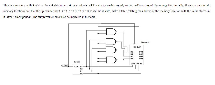
This is a memory with 4 address bits, 4 data inputs, 4 data outputs, a CE memory enable signal, and a read/write signal. Assuming that, initially, 0 was written in all memory locations and that the up counter has Q3 = Q2 = Q1 = Q0 = 0 as its initial state, make a table relating the address of the memory location with the value stored in it, after 8 clock periods. The output values must also be indicated in the table. CLOCK Count CLK 03 02 01 00 013 012 DH DID CE RW Memory D03 DO2 D01 BOO A3 A2 A1 AD
Step by Step Solution
3.32 Rating (146 Votes )
There are 3 Steps involved in it
The image shows a memory module with 4 address bits 4 data inputs 4 data outputs a CE Chip Enable me... View full answer

Get step-by-step solutions from verified subject matter experts