

Question: Time propagation delay in logic diagram How is time propagation delay calculated?? How was the time propagation delay in the example below calculated? For timing
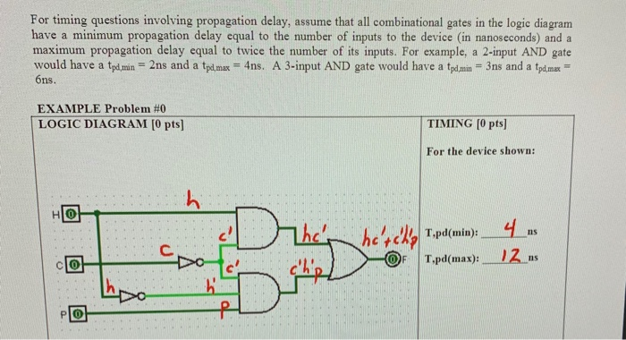
For timing questions involving propagation delay, assume that all combinational gates in the logic diagram have a minimum propagation delay equal to the number of inputs to the device (in nanoseconds) and a maximum propagation delay equal to twice the number of its inputs. For example, a 2-input AND gate would have a tpd.min 2ns and a tpdmax 4ns. A 3-input AND gate would have a tpdmin 3ns and a tpdmax 6ns. EXAMPLE Problem #0 LOGIC DIAGRAM [0 pts] TIMING (0 pts For the device shown: H C. OF T.pd(mas): 12 ns For timing questions involving propagation delay, assume that all combinational gates in the logic diagram have a minimum propagation delay equal to the number of inputs to the device (in nanoseconds) and a maximum propagation delay equal to twice the number of its inputs. For example, a 2-input AND gate would have a tpd.min 2ns and a tpdmax 4ns. A 3-input AND gate would have a tpdmin 3ns and a tpdmax 6ns. EXAMPLE Problem #0 LOGIC DIAGRAM [0 pts] TIMING (0 pts For the device shown: H C. OF T.pd(mas): 12 ns
Step by Step Solution
There are 3 Steps involved in it

Get step-by-step solutions from verified subject matter experts