

Question: Using VHDL language, ALTERA Quartus II software and ALTERA DE2-115 board, you should design, simulate and implement an 8-bit bi-directional shift register with parallel load.
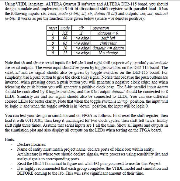
Using VHDL language, ALTERA Quartus II software and ALTERA DE2-115 board, you should design, simulate and implement an 8-bit bi-directional shift register with parallel load. It has the following inputs: clk, reset, mode (2-bit), sil, sir, datain (8-bit) and outputs sol, sor, dataout (8-bit). It works as per the function table given below (where +ve denotes positive) reset modeclkoperation aataout : sh ht 0 / 10 / +ve edge dataout : datain 01 ve edge Note that sil and sir are serial inputs for left shift and right shift respectively, similarly sol and sor are serial outputs. The mode input should be given by toggle switches on the DE2-115 board. The reset, sil and sir signal should also be given by toggle switches on the DE2-115 board. For simplicity, use a push button to give the clock (clk) signal. Notice that because the push buttons are inverted, when pressing down a push button you will generate a negative clock edge, and when releasing the push button you will generate a positive clock edge. The 8-bit parallel input datain should be controlled by 8 toggle switches, and the S-bit output dataout should be connected to 8 LEDs. Similarly sol and sor signal should also be connected to LEDs. You can use different colored LEDs for better clarity. Note that when the toggle switch is in "up" position, the input will be logic 1 and when the toggle switch is in "down" position, the input will be logic 0 You can test your design in simulator and on FPGA as follows: First reset the shift register, then load it with 00110101; then keep it unchanged for two clock cycles, then shift left twice; finally shift right three times. Assume that serial inputs are 1 all the time. Show all inputs and outputs in the simulation plot and also display all outputs on the LEDs when testing on the FPGA board. Hints: Declare libraries. Name of entity must match project name, declare ports of black box within entity, Archutecture is where you should declare signals, wnte processes using sensitivity list, and assign signals to corresponding ports. Read the DE2-115 manual to figure out what I/O pins you need to use for this Project. It is highly recommended that each group completes the VHDL model and simulation and BEFORE coming to the lab. This will save significant amount of their time - Using VHDL language, ALTERA Quartus II software and ALTERA DE2-115 board, you should design, simulate and implement an 8-bit bi-directional shift register with parallel load. It has the following inputs: clk, reset, mode (2-bit), sil, sir, datain (8-bit) and outputs sol, sor, dataout (8-bit). It works as per the function table given below (where +ve denotes positive) reset modeclkoperation aataout : sh ht 0 / 10 / +ve edge dataout : datain 01 ve edge Note that sil and sir are serial inputs for left shift and right shift respectively, similarly sol and sor are serial outputs. The mode input should be given by toggle switches on the DE2-115 board. The reset, sil and sir signal should also be given by toggle switches on the DE2-115 board. For simplicity, use a push button to give the clock (clk) signal. Notice that because the push buttons are inverted, when pressing down a push button you will generate a negative clock edge, and when releasing the push button you will generate a positive clock edge. The 8-bit parallel input datain should be controlled by 8 toggle switches, and the S-bit output dataout should be connected to 8 LEDs. Similarly sol and sor signal should also be connected to LEDs. You can use different colored LEDs for better clarity. Note that when the toggle switch is in "up" position, the input will be logic 1 and when the toggle switch is in "down" position, the input will be logic 0 You can test your design in simulator and on FPGA as follows: First reset the shift register, then load it with 00110101; then keep it unchanged for two clock cycles, then shift left twice; finally shift right three times. Assume that serial inputs are 1 all the time. Show all inputs and outputs in the simulation plot and also display all outputs on the LEDs when testing on the FPGA board. Hints: Declare libraries. Name of entity must match project name, declare ports of black box within entity, Archutecture is where you should declare signals, wnte processes using sensitivity list, and assign signals to corresponding ports. Read the DE2-115 manual to figure out what I/O pins you need to use for this Project. It is highly recommended that each group completes the VHDL model and simulation and BEFORE coming to the lab. This will save significant amount of their time
Step by Step Solution
There are 3 Steps involved in it

Get step-by-step solutions from verified subject matter experts