

Question: You are asked to implement a chip t ester for the 74 LS 138 3x8 decoder chip shown in the figure bclow by in- terfacing
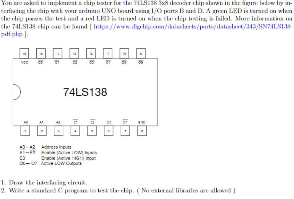
You are asked to implement a chip t ester for the 74 LS 138 3x8 decoder chip shown in the figure bclow by in- terfacing the chip with your arduio UNO board usg I/O ports B and D. A green LED is turned on when the chip passes the test and a red LED is turned on when the chip testing is failed. More information on the 74LS138 chip can be found https://www.digchip.com/datashcets/parts/datashet/343/SN74LS138- pdf.php] 18 14 13 12 10 voo ?? 02 03 04 05 06 74LS138 AO A1 E1 E2 ?? 07 GND A0-A2 Address Inputs E1-E2 Enable (Active LOW) Inputs ?? 00-07 Active LOW Outputs Enable (Active HIGH) Input 1. Draw the interfacing circuit. 2. Write a standard C program to test the chip. (No external librarics are allowed You are asked to implement a chip t ester for the 74 LS 138 3x8 decoder chip shown in the figure bclow by in- terfacing the chip with your arduio UNO board usg I/O ports B and D. A green LED is turned on when the chip passes the test and a red LED is turned on when the chip testing is failed. More information on the 74LS138 chip can be found https://www.digchip.com/datashcets/parts/datashet/343/SN74LS138- pdf.php] 18 14 13 12 10 voo ?? 02 03 04 05 06 74LS138 AO A1 E1 E2 ?? 07 GND A0-A2 Address Inputs E1-E2 Enable (Active LOW) Inputs ?? 00-07 Active LOW Outputs Enable (Active HIGH) Input 1. Draw the interfacing circuit. 2. Write a standard C program to test the chip. (No external librarics are allowed
Step by Step Solution
There are 3 Steps involved in it

Get step-by-step solutions from verified subject matter experts