

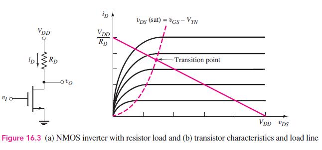
(a) Redesign the resistive load inverter in Figure 16.3 (a) so that the maximum power dissipation is...
Question:
(a) Redesign the resistive load inverter in Figure 16.3 (a) so that the maximum power dissipation is \(0.25 \mathrm{~mW}\) with \(V_{D D}=3.3 \mathrm{~V}\) and \(v_{O}=0.15 \mathrm{~V}\) when the input is a logic 1 .
(b) Using the results of part (a), what is the input voltage range when the transistor is biased in the saturation region?
Fantastic news! We've Found the answer you've been seeking!
Step by Step Answer:

Answered By
Muhammad Umair
I have done job as Embedded System Engineer for just four months but after it i have decided to open my own lab and to work on projects that i can launch my own product in market. I work on different softwares like Proteus, Mikroc to program Embedded Systems. My basic work is on Embedded Systems. I have skills in Autocad, Proteus, C++, C programming and i love to share these skills to other to enhance my knowledge too.
1+ Reviews
10+ Question Solved
Related Book For 

Microelectronics Circuit Analysis And Design
ISBN: 9780071289474
4th Edition
Authors: Donald A. Neamen
Question Posted:
