

Consider the MOSFET diff-amp with the configuration in Figure P11.33. The circuit parameters are (V^{+}=3 mathrm{~V}, V^{-}=-3
Question:
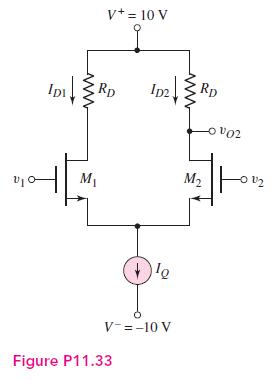
Consider the MOSFET diff-amp with the configuration in Figure P11.33. The circuit parameters are \(V^{+}=3 \mathrm{~V}, V^{-}=-3 \mathrm{~V}\), and \(I_{Q}=0.2 \mathrm{~mA}\). The transistor parameters are \(V_{T N}=0.4 \mathrm{~V}\), \(k_{n}^{\prime}=100 \mu \mathrm{A} / \mathrm{V}^{2}, W / L=10\), and \(\lambda=0\). The range of the commonmode input voltage is to be \(-1.5 \leq v_{c m} \leq+1.5 \mathrm{~V}\), and the commonmode rejection ratio is to be \(\mathrm{CMRR}_{\mathrm{dB}}=50 \mathrm{~dB}\).
(a) Design the diff-amp to produce the maximum possible differential-mode voltage gain.
(b) Design an all MOSFET current source to produce the desired bias current and CMRR. The minimum \(W / L\) ratio of any transistor is to be 0.8 , and assume \(\lambda=0.02 \mathrm{~V}^{-1}\) for all transistors in the current source circuit.
Step by Step Answer:


Microelectronics Circuit Analysis And Design
ISBN: 9780071289474
4th Edition
Authors: Donald A. Neamen
