

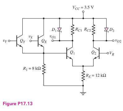
In the circuit in Figure P17.13, the input voltages (v_{X}) and (v_{Y}) are compatible with the output
Question:
In the circuit in Figure P17.13, the input voltages \(v_{X}\) and \(v_{Y}\) are compatible with the output voltages \(v_{O 1}\) and \(v_{O 2}\). Neglect base currents.
(a) Design an appropriate value of \(V_{R}\). State the reason for your selection.
(b) Determine the value of \(R_{C 1}\) such that, when \(Q_{1}\) is on, the current in \(R_{C 1}\) is one-half that in \(D_{1}\).
(c) Determine the value of \(R_{C 2}\) such that, when \(Q_{2}\) is on, the current in \(R_{C 2}\) is one-half that in \(D_{2}\).
(d) Calculate the power dissipated in the circuit when \(v_{X}=v_{Y}=\operatorname{logic} 0\).
Fantastic news! We've Found the answer you've been seeking!
Step by Step Answer:

Answered By
Utsab mitra
I have the expertise to deliver these subjects to college and higher-level students. The services would involve only solving assignments, homework help, and others.
I have experience in delivering these subjects for the last 6 years on a freelancing basis in different companies around the globe. I am CMA certified and CGMA UK. I have professional experience of 18 years in the industry involved in the manufacturing company and IT implementation experience of over 12 years.
I have delivered this help to students effortlessly, which is essential to give the students a good grade in their studies.
2+ Reviews
10+ Question Solved
Related Book For 

Microelectronics Circuit Analysis And Design
ISBN: 9780071289474
4th Edition
Authors: Donald A. Neamen
Question Posted:
