

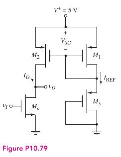
The bias voltage of the MOSFET amplifier with active load in Figure (mathrm{P} 10.79) is changed to
Question:
The bias voltage of the MOSFET amplifier with active load in Figure \(\mathrm{P} 10.79\) is changed to \(V^{+}=3 \mathrm{~V}\). The transistor parameters are \(V_{T N}=\) \(0.5 \mathrm{~V}, V_{T P}=-0.5 \mathrm{~V}, k_{n}^{\prime}=100 \mu \mathrm{A} / \mathrm{V}^{2}, k_{p}^{\prime}=60 \mu \mathrm{A} / \mathrm{V}^{2}\), and \(\lambda_{n}=\lambda_{p}=\) \(0.02 \mathrm{~V}^{-1}\). The quiescent values are \(V_{O}=1.5 \mathrm{~V}\) and \(V_{I}=1.2 \mathrm{~V}\).
(a) Design the circuit \(W / L\) ratios, such that \(I_{\mathrm{REF}}=I_{O}=100 \mu \mathrm{A}\). Assume \(M_{1}\) and \(M_{2}\) are matched.
(b) Determine the small-signal voltage gain.
Fantastic news! We've Found the answer you've been seeking!
Step by Step Answer:

Answered By
Mahesh G
I have more than 7 years of experience in teaching physics, mathematics and python programming to more than 600 students including both online and offline tutoring.
I follow the following 7 step fundamental approach towards tutoring.
1. Curiosity, scope, enlightenment of the topic in hand.
2. Problem Definitions and elaboration.
3. Requisite mathematics, analytical abilities and quantitative
aptitude.
4. Preparing Algorithms for problem statement.
5. Concepts with analogies and building algorithm.
6. Introspection and improvising.
7. Daily class wise Cheat sheets(its not cheating) for consolidation.
1+ Reviews
10+ Question Solved
Related Book For 

Microelectronics Circuit Analysis And Design
ISBN: 9780071289474
4th Edition
Authors: Donald A. Neamen
Question Posted:
