

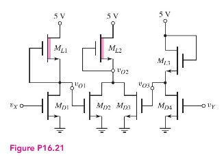
The transistor parameters for the circuit in Figure P16.21 are: (V_{T N}=0.8 mathrm{~V}) for all enhancement-mode devices,
Question:
The transistor parameters for the circuit in Figure P16.21 are: \(V_{T N}=0.8 \mathrm{~V}\) for all enhancement-mode devices, \(V_{T N}=-2 \mathrm{~V}\) for the depletion-mode devices, and \(k_{n}^{\prime}=60 \mu \mathrm{A} / \mathrm{V}^{2}\) for all devices. The width-to-length ratios of \(M_{L 2}\) and \(M_{L 3}\) are 1 , and those for \(M_{D 2}, M_{D 3}\), and \(M_{D 4}\) are 8.
(a) For \(v_{X}=5 \mathrm{~V}\), output \(v_{O 1}\) is \(0.15 \mathrm{~V}\), and the power dissipation in this inverter is to be no more than \(250 \mu \mathrm{W}\). Determine ( \(W / L)_{M L 1}\) and ( \(\left.W / L\right)_{M D 1}\).
(b) For \(v_{X}=v_{Y}=0\), determine \(v_{O 2}\).
Fantastic news! We've Found the answer you've been seeking!
Step by Step Answer:

Answered By
Muhammad Umair
I have done job as Embedded System Engineer for just four months but after it i have decided to open my own lab and to work on projects that i can launch my own product in market. I work on different softwares like Proteus, Mikroc to program Embedded Systems. My basic work is on Embedded Systems. I have skills in Autocad, Proteus, C++, C programming and i love to share these skills to other to enhance my knowledge too.
1+ Reviews
10+ Question Solved
Related Book For 

Microelectronics Circuit Analysis And Design
ISBN: 9780071289474
4th Edition
Authors: Donald A. Neamen
Question Posted:
