

Question: Consider a four-input NMOS NOR logic gate with a depletion load similar to the circuit in Figure P16.19. Assume (V_{D D}=2.5 mathrm{~V}, V_{T N D}=0.4
Consider a four-input NMOS NOR logic gate with a depletion load similar to the circuit in Figure P16.19. Assume \(V_{D D}=2.5 \mathrm{~V}, V_{T N D}=0.4 \mathrm{~V}\), and \(V_{T N L}=-0.6 \mathrm{~V}\). The maximum value of \(v_{O}\) in its low state is to be \(50 \mathrm{mV}\).
(a) Determine \(K_{D} / K_{L}\).
(b) The maximum power dissipation in this NOR logic gate is to be \(50 \mu \mathrm{W}\). Determine the width-to-length ratio of each transistor.
(c) Determine \(v_{O}\) when (i) two inputs are a logic 1, (ii) three inputs are a logic 1 , and (iii) all inputs are a logic 1 .
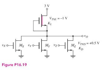
x o 3V VTNI=-1 V K. My by My "zo Mz Kp Figure P16.19 010 VIND +0.5 V =
Step by Step Solution
3.36 Rating (162 Votes )
There are 3 Steps involved in it

Get step-by-step solutions from verified subject matter experts